Sensor-type package and method for fabricating the same

a sensor-type package and sensor-type technology, applied in the field of semiconductor packages, can solve the problems of not only bulky but also expensive, and cannot be further reduced to improve the electrical properties so as to avoid the problems of high cost, high cost and possible contamination, and high-integration of the sensor-type package.

Inactive Publication Date: 2009-02-12
SILICONWARE PRECISION IND CO LTD
View PDF6 Cites 98 Cited by
  • Summary
  • Abstract
  • Description
  • Claims
  • Application Information

AI Technical Summary

Benefits of technology

[0011]It is another objective of this invention to provide an easily fabricated, low cost sensor-type package and a method for fabricating the same.
[0014]It is yet another objective of this invention to provide a sensor-type package, whereby contamination due to uses of high-molecular adhesive layers is avoided or uses supports, and a method for fabricating the same.
[0018]Moreover, the grooves can be filled (but not the sensing areas) with an insulative material to effectively fix the sensor chips in the grooves; a plurality of passive components can be further mounted in the grooves to enhance overall electrical quality of the sensor-type package. Furthermore, a lens mount can be disposed on one side of the sensor-type package corresponding to the transparent cover.
[0022]By doing so, a wafer-level process is completed, such that light, thin, short, small and highly integrated sensor-type packages are formed. The aforesaid wafer-level process can provide a light, thin, short and small sensor-type package. Additionally, sensor chips having TSV are stacked and electrically connected to DSP control units disposed with TSV to provide a highly integrated sensor-type package. At the same time, the invention uses the unlaminated wafer (having a plurality of semiconductor chips) as supporting carriers in the processes, so as to avoid the problems of complexity of processes, high costs and possible contamination caused by applying the TSV technique, as used in the prior arts, to perpendicularly stack a plurality of chips and use supports and adhesive layers for multiple times to mount the chips on the chip carriers.

Problems solved by technology

However, such sensor-type packages are limited by the needs to have at least sufficient space for disposing the dam structure on the chip carrier.
As such, sizes of the sensor-type packages are limited by dam structures and distributions of bonding wires, such that they cannot be further reduced to improve electrical properties of the sensor-type packages.
This is a package at package-level, which is not only bulky but also expensive.
Moreover, control units such as digital signal processors (DSP) cannot be integrated in the sensor-type package.
Therefore, the sensor-type package cannot meet the demands of lightness, thinness, shortness, smallness and high degrees of integration from the industry.
However, in the aforesaid process, the additional use of a plurality of supports 251 and 252, along with the adhesion of the first wafer 21a and the second wafer 22a for multiple times on the supports 251 and 252, not only increase production costs, but also raise complexity of processes.
Furthermore, if the adhesive layers 241 and 242 are high-molecular materials such as epoxy resins, sputtering and stripping processes typically used to form the bond pads 231 and 236 are extremely likely to cause contaminations that leading to lowered productions.
Accordingly, the prior arts, which use the TSV technique to provide a plurality of semiconductor chips stacked and interconnected to form a MCM, cannot be effectively applied to sensor-type packages.

Method used


Image

  • Sensor-type package and method for fabricating the same
  • Sensor-type package and method for fabricating the same
  • Sensor-type package and method for fabricating the same

Examples


first embodiment

[0030]Referring to FIGS. 3A through 3F, FIGS. 3A through 3F are schematic diagrams of a sensor-type package and a method for fabricating the same according to the first embodiment of the invention.

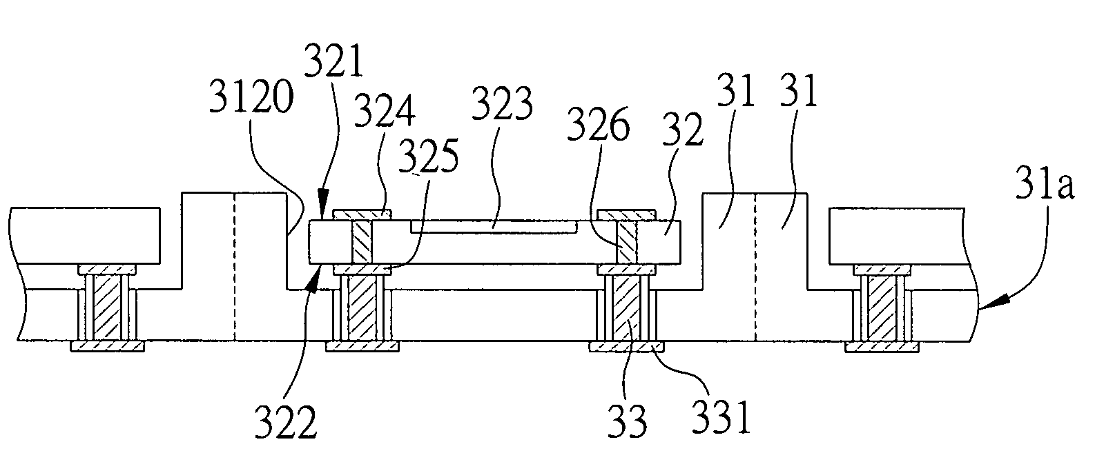
[0031]As shown in FIG. 3A, a wafer 31a containing a plurality of semiconductor chips 31a (such as DSP) are provided. The wafer 31a and each of the semiconductor chips 31 have a first surface 311 and a second surface 312 opposite to the first surface 311, wherein a plurality of holes 310 are formed over the first surface 311 of the semiconductor chips 31, to form a plurality of metallic pillars 33 and bond pads 331, respectively, in and on the holes 310 to form a TSV.

[0032]A silicon dioxide or silicon nitride insulative layer 33″ is disposed between the holes 310 and the metallic pillars 33 of the TSV, and a nickel barrier layer 33′ is disposed between the insulative layer 33″ and the metallic pillars 33. Materials of the metallic pillars can be, for example, one of copper, gold, aluminum, ...

second embodiment

[0041]Referring to FIG. 4, FIG. 4 is a schematic diagram of a sensor-type package and a method for fabricating the same according to the second embodiment of the invention. For simplicity, identical or similar components are represented by the same symbol.

[0042]The sensor-type package and the method for fabricating the same, of the embodiment, is substantially the same as the ones described in the first embodiment. The major difference is that the insulative material 34 is filled in the groove 3120 (but not the sensing area 323 of the sensor chip 32) on the second surface 312 of each of the semiconductor chips 31 of the wafer 31a, so as to effectively fix the sensor chip 32 in the groove 3120.

third embodiment

[0043]Referring to FIG. 5, FIG. 5 is a schematic diagram of a sensor-type package and a method for fabricating the same according to the third embodiment of the invention. For simplicity, identical or similar components are represented by the same symbol.

[0044]The sensor-type package and a method for fabricating the same, of the embodiment, is substantially the same as the ones described in the first embodiment. The major difference is that the passive components 38 can be further mounted onto and electrically connected to the groove 3120 on the second surface 312 of the semiconductor chips 31, so as to enhance the electrical property of the sensor-type package.


PUM


Abstract

A sensor-type package and a method for fabricating the same are provided. A wafer having a plurality of semiconductor chips is provided, wherein a plurality of holes are formed on a first surface of each of the semiconductor chips, and a plurality of metallic pillars formed in the holes and a plurality of bond pads connected to the metallic pillars form through silicon vias (TSVs). A groove is formed on a second surface of each of the semiconductor chips to expose the metallic pillars. A plurality of sensor chips having TSVs are stacked in the grooves of the semiconductor chips and electrically connected to the exposed metallic pillars. A transparent cover is mounted onto the second surfaces of the semiconductor chips to cover the grooves. A plurality of conductive components are implanted on the bond pads of the semiconductor chips. The wafer is cut along borders among the semiconductor chips.

Description

BACKGROUND OF THE INVENTION[0001]1. Field of the Invention[0002]The present invention relates to semiconductor packages and methods for fabricating the same, and more particularly, to a sensor-type package and a method for fabricating the sensor-type package.[0003]2. Description of the Prior Art[0004]Conventional image sensor packages, such as the ones disclosed in U.S. Pat. Nos. 6,060,340, 6,262,479 and 6,590,269, prepare a dam structure on a chip carrier, before receiving and wire-bonding a sensor chip to the space defined by the dam structure on the chip carrier and attaching a transparent glass on the dam structure to cover the space. However, such sensor-type packages are limited by the needs to have at least sufficient space for disposing the dam structure on the chip carrier. At the same time, the sensor-type packages are required to be electrically connected to the chip carrier via bonding wires. As such, sizes of the sensor-type packages are limited by dam structures and di...

Claims


Application Information

Patent Timeline
Patent Type & Authority Applications(United States)
IPC IPC(8): H01L23/52H01L21/00
CPCH01L27/14618H01L2224/13H01L27/14683H01L27/14625H01L2224/13025H01L2224/05001H01L2224/056H01L2924/19105H01L2224/97H01L2924/19104H01L2224/94H01L2224/16146H01L2924/00014H01L2224/81H01L2224/83
Inventor CHAN, CHANG-YUEHHUANG, CHIEN-PINGCHANG, TSE-WENCHANG, CHIN-HUANGHUANG, CHIH-MING
Owner SILICONWARE PRECISION IND CO LTD
Why Eureka
Try Eureka