Semiconductor device

a semiconductor device and semiconductor technology, applied in the field of semiconductor devices, can solve the problems of easy contact with the void, invading metal materials, and sometimes displaced via hole h from the center of the contact region, and achieve the effect of high reliability and higher yield of the semiconductor devi

Inactive Publication Date: 2009-02-19
POWERCHIP SEMICON CORP +1
View PDF2 Cites 6 Cited by
  • Summary
  • Abstract
  • Description
  • Claims
  • Application Information

AI Technical Summary

Benefits of technology

[0022]According to the embodiment, any void does not exist in the interlayer insulation film located between the contacting portion of the via hole and the interconnection line adjacent thereto, thereby reliably preventing any

Problems solved by technology

However, in the prior art, a void exists on the lateral side of the via contact section, and therefore when a via hole is displaced, it may easily come into contact with the void.
This inevitably causes such problems as invasion of metal materials and intrusion of polymer cleaning liquid into the aforementioned void.
Meanwhile, the via hole H is sometimes displaced from the center of the contact region due to, e.g., mask alignment error during lithography process.
If the via hole H is greatly displaced to come into contact with the void V in between interconnection lines as shown in FIG. 7B, metal materials of the via hole (such as Ti, TiN, W, etc. in ca

Method used


Image

  • Semiconductor device
  • Semiconductor device
  • Semiconductor device

Examples


embodiment 1

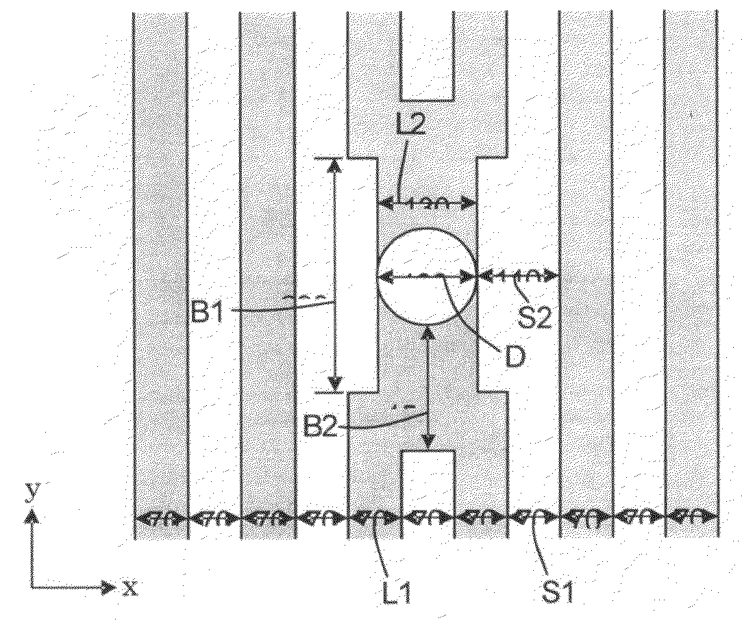
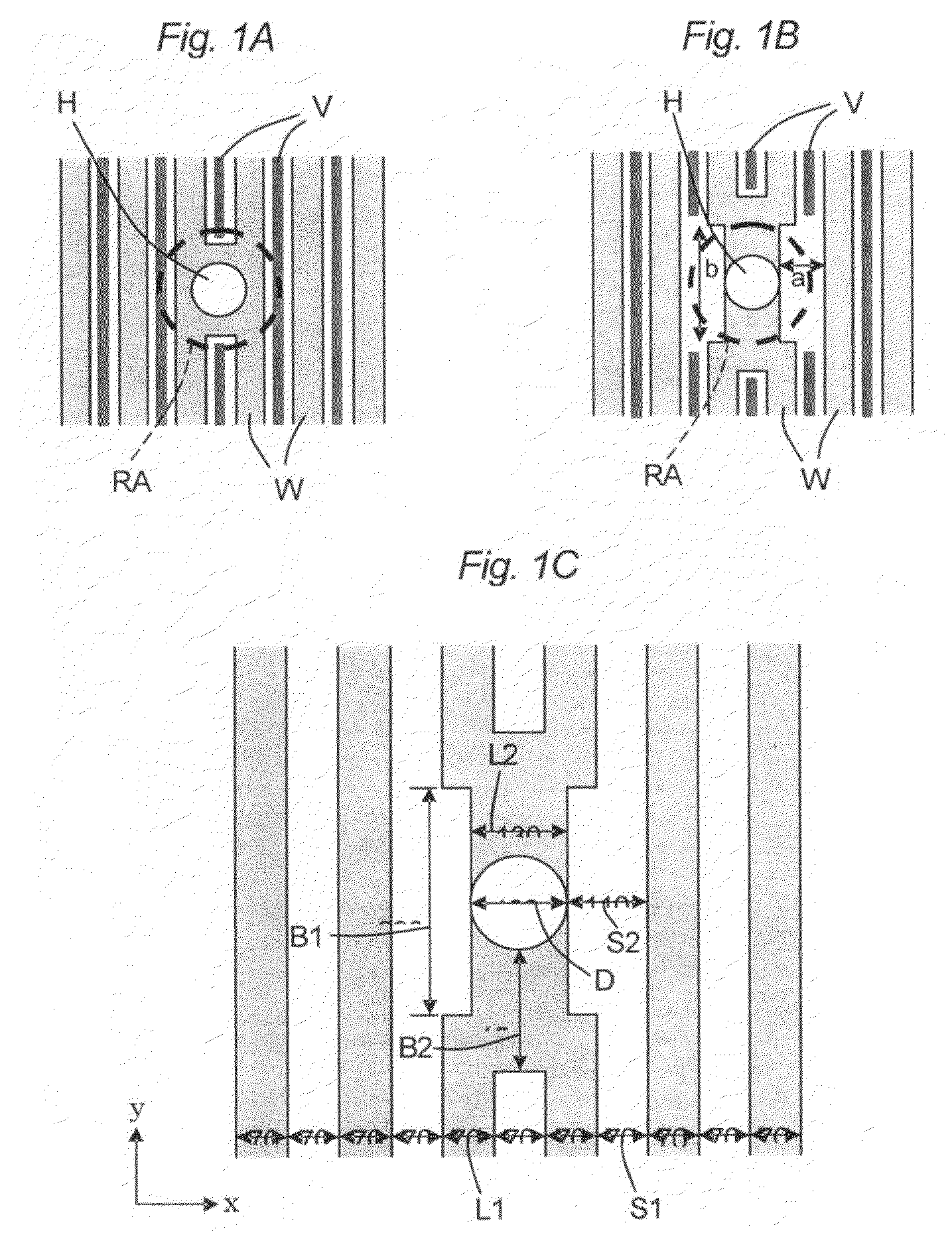
[0032]FIG. 1A is a plan view showing an example of layout of a conventional interconnection pattern as a comparative example. FIG. 1B is a plan view showing an example of layout of an interconnection pattern according to an embodiment of the invention, and FIG. 1C is an enlarged view of FIG. 1B.

[0033]Hereinafter, layout of the interconnection pattern in a flash memory will be explained by way of example, the invention can be applied to various kinds of semiconductor integrated circuits, such as DRAM, SRAM, ROM and SoC.

[0034]Since semiconductor integrated circuits generally have a plurality of interconnection layers, with the lowermost interconnection layer nearest to a semiconductor substrate having the highest interconnection density, the most critical dimensional and positional accuracy are required for the lowermost interconnection layer. An interlayer insulation film is embedded in between the lower interconnection layer and the upper interconnection layer, and a via hole H is f...

embodiment 2

[0066]FIGS. 6A to 6F are plan views showing various examples of layouts of interconnection patterns in the contact region and adjacent regions thereof according to the invention. First, in FIG. 6A, the shape of the notch in the contact region to which the via hole H is connected is the same as that of FIG. 1B, whereas the joint portion of the two interconnection lines W for forming the contact region is longer than that of FIG. 1B.

[0067]In FIG. 6B, the shape of the notch in the contact region to which the via hole H is connected is the same as that of FIG. 1B, whereas two or more interconnection lines W adjacent to the contact region are joined to each other, in which other notches are provided so as to face the notches in the contact region, respectively.

[0068]In FIG. 6C, two or more interconnection lines W adjacent to the contact region to which the via hole H is connected are joined to each other, and the contact region is not provided with any notches but the adjacent interconne...


PUM


Abstract

A semiconductor device includes: an interlayer insulation film; a lower interconnection layer; an upper interconnection layer; and a via hole extending through the interlayer insulation film to establish electric connection between the lower and upper interconnections; wherein a plurality of interconnection lines is provided in the lower interconnection layer, and a contact region is formed for contact with the via hole by partially joining at least two interconnection lines, and a void exists in a first region of the interlayer insulation film located between adjacent interconnection lines, and no void exists in a second region of the interlayer insulation film located between a contacting portion of the via hole in the contact region and an interconnection line adjacent to the contact region, whereby reliably preventing any contact between a via hole and a void formed in an interlayer insulation film even when the via hole is greatly displaced.

Description

BACKGROUND OF THE INVENTION[0001]1. Field of the Invention[0002]The present invention relates to a semiconductor device, for example, a semiconductor integrated circuit including highly-dense interconnection patterns, such as DRAM (Dynamic Random Access Memory), SRAM (Static Random Access Memory), ROM (Read Only Memory), flash memory and SoC (System-on-Chip).[0003]2. Description of the Related Art[0004]Prior art (JP-11-307531A (1999)) refers to voids generated in interlayer insulation films as interconnections is further minimized. More specifically, narrower interconnections other than those of via contact sections are formed so as to suppress generation of voids, and also the volume of the voids in an entire IC is reduced so as to prevent burst failure of IC which may be caused by void swelling during heat treatment in manufacturing IC.[0005]However, in the prior art, a void exists on the lateral side of the via contact section, and therefore when a via hole is displaced, it may e...

Claims


Application Information

Patent Timeline
IPC IPC(8): H01L23/48
CPCH01L23/5226H01L23/528H01L2924/0002H01L2924/00
Inventor ABE, SATOSHI
Owner POWERCHIP SEMICON CORP
Why Eureka
Try Eureka