Film forming method of porous film and computer-readable recording medium

a film forming method and film technology, applied in the direction of coatings, metallic material coating processes, chemical vapor deposition coatings, etc., can solve the problems of difficult reproducibility of modifying processes, unwanted increase of specific dielectric constants, etc., to suppress the shrinkage of dielectric films, suppress the increase of dielectric films density, and increase the density of dielectric films

Inactive Publication Date: 2009-02-26
TOKYO ELECTRON LTD
View PDF11 Cites 28 Cited by
  • Summary
  • Abstract
  • Description
  • Claims
  • Application Information

AI Technical Summary

Benefits of technology

[0019]According to the present invention, the organic functional groups generally designated as CHx, such as CH3, C2H5, . . . , or the hydroxyl group (OH) contained in the dielectric film is discharged to the outside of the film with a controlled rate in the pore forming step, by carrying out the film formation of the porous film by the steps of: forming the dielectric film containing an organic functional group and a hydroxyl group on a substrate by an organic silicon compound source; forming a surface densification layer having a higher density than a main part of the dielectric film on a surface of the dielectric film by carrying out a densification processing removing the organic functional group and the hydroxyl group; and forming pores in the main part of the dielectric film by exposing the dielectric film formed with the surface densification layer to the hydrogen radicals excited by plasma such that the organic functional group and the hydroxyl group are removed. Thereby, it becomes possible to suppress the shrinkage of the dielectric film at the time of the pore forming step effectively. As a result, increase of density of the dielectric film is suppressed and it becomes possible to obtain a dielectric film of low dielectric constant.
[0020]Further, by shutting off the film forming source gas alone, after the film forming process, while continuing the supply of the plasma gas and the oxidizing gas and further continuing the supply of the plasma power, formation of particles at the end of the film forming process is effectively suppressed, and it becomes possible to improve the yield of film formation significantly.

Problems solved by technology

However, with such an approach of modifying the SiOCH film formed on a substrate by applying thereto the hydrogen plasma processing, it becomes necessary to carry out delicate control during the modifying process, and it has been difficult to carry out the modifying process with reproducibility in mass production line.
However, with such conventional modification process, there tends to occur contraction rather than the dilatation in the SiOCH film in the case the process condition of the modification processing falls outside the optimum range, and there may be caused unwanted increase of specific dielectric constant in the film as a result of increase of density associated with the contraction.Patent Reference 1 WO2005 / 045916Patent Reference 2 Japanese Laid-Open Patent Application 2003-503849Non-Patent Reference 1 A. Grill and D. A. Neumayer, J. Appl. Phys. vol.

Method used


Image

  • Film forming method of porous film and computer-readable recording medium
  • Film forming method of porous film and computer-readable recording medium
  • Film forming method of porous film and computer-readable recording medium

Examples


first embodiment

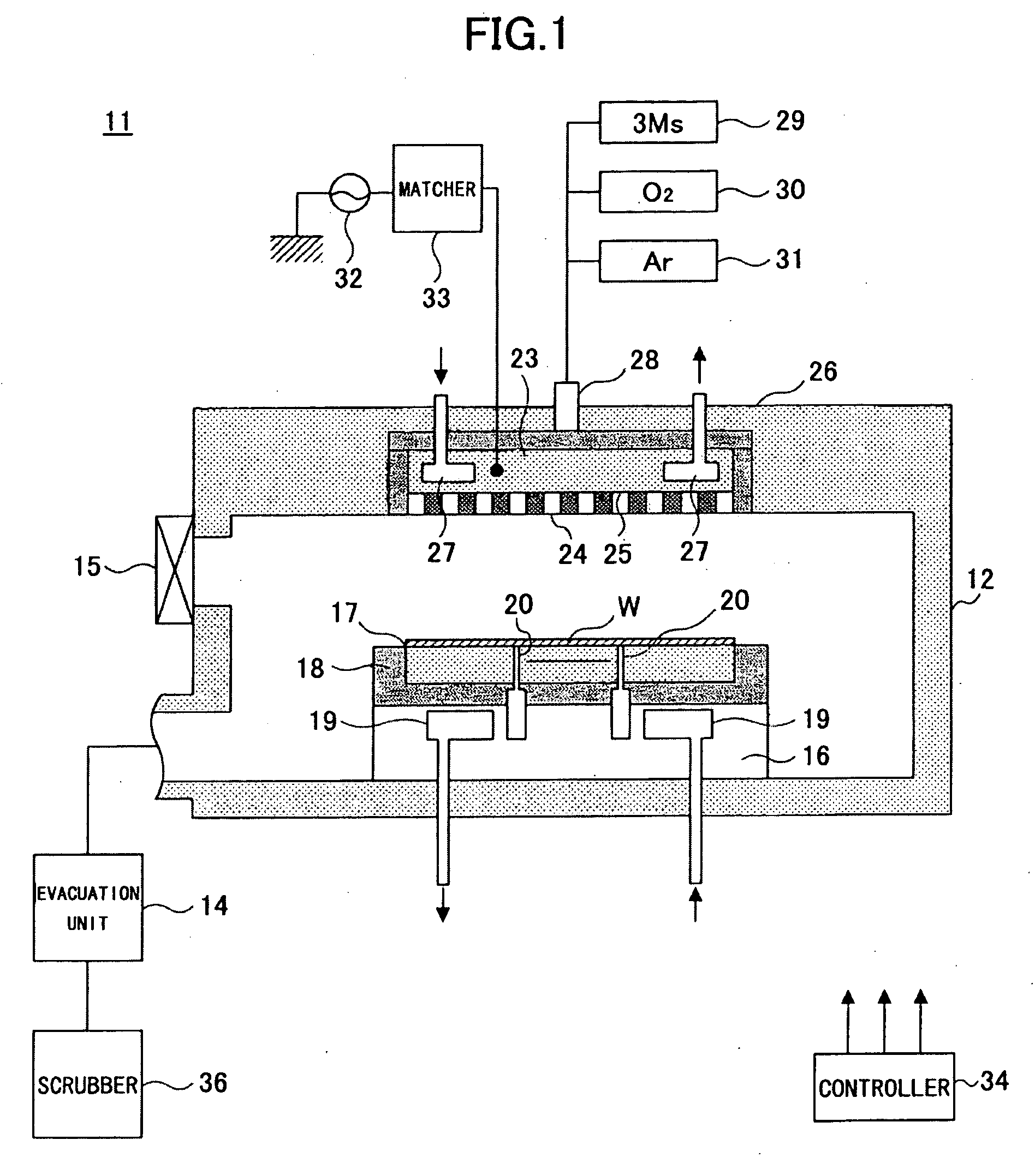
[0046]FIG. 1 shows the construction of a parallel-plate type substrate processing apparatus 11 used for the film forming processing of dielectric film with the present invention.

[0047]Referring to FIG. 1, the substrate processing apparatus 11 includes a processing vessel 12 formed of a conductive material such as anodized aluminum, wherein the processing vessel 12 is evacuated by an evacuation apparatus 14 such as a turbo molecular pump via an evacuation port 13, and there is provided a susceptor 17 inside the processing vessel 12 in a matter supported by a susceptor support base 16 of generally cylindrical shape. The susceptor 17 holds thereon a substrate W to be processed. The susceptor 17 functions also as the lower electrode of the parallel plate substrate processing apparatus 11, and there is provided an insulator 18 of ceramic or the like between the susceptor support base 16 and the susceptor 17. Further, the processing vessel 12 is grounded.

[0048]In the interior of the susce...

second embodiment

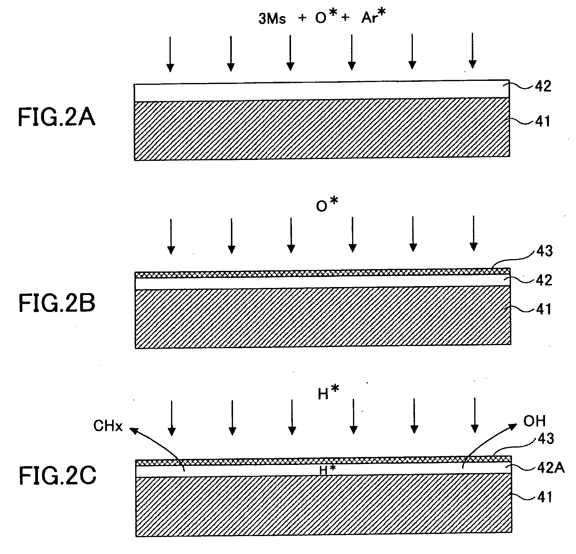
[0105]FIGS. 10A-10D show a film forming method according to a second embodiment of the present invention. In the drawings, those parts explained before are designated by the same reference numerals and the description thereof will be omitted.

[0106]Referring to FIGS. 10A-10D, it will be noted that the processes of FIGS. 10A-10C are identical to those of FIGS. 2A-2C noted before, while the present embodiment further processes the structure obtained with the process of FIG. 10C with plasma excited oxygen radicals O* or oxygen radicals O* and hydrogen radicals H* in the process of FIG. 10D.

[0107]For example, the structure obtained with the process of FIG. 10C is processed in the same microwave plasma processing apparatus at the same substrate temperature (such as 400° C.) while setting the processing pressure to generally the same processing pressure of 20-1333 Pa, preferably 20-650 Pa such as 260 Pa, for example, and by supplying the Ar gas with the flow rate of 250 SCCM and the oxygen...

third embodiment

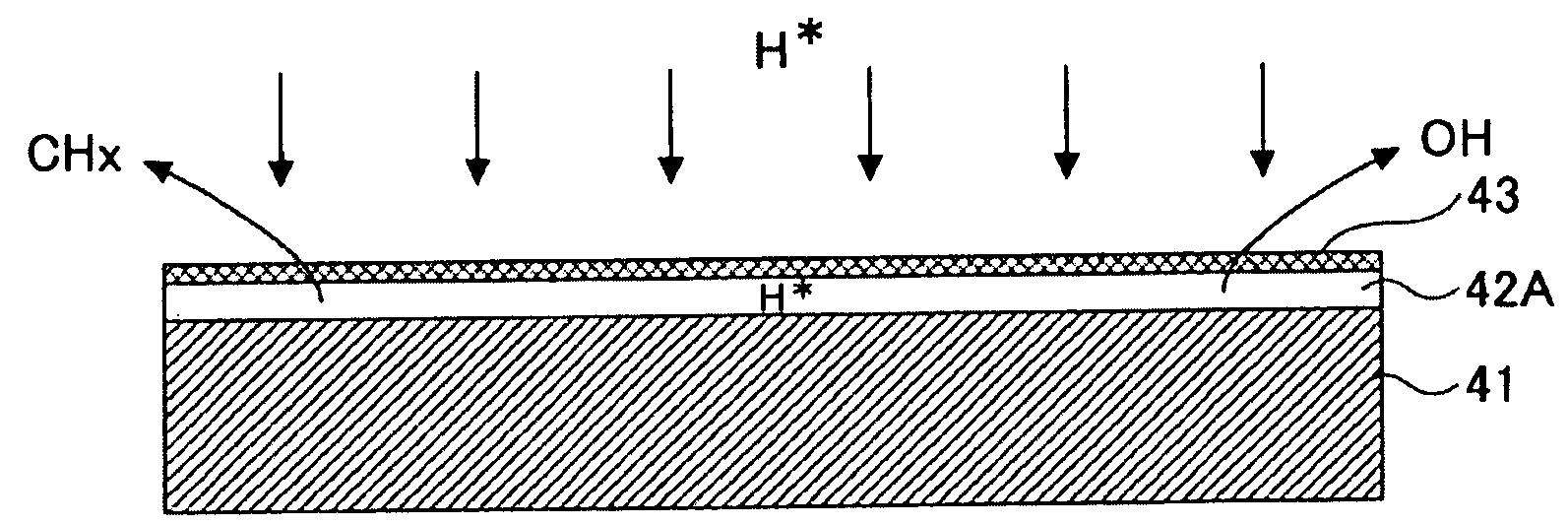
[0145]In the embodiments explained previously, it will be noted that the densification layer 43 remains on the porous SiOCH film 42A. Thereby, it is preferable to remove the densification layer 43 because such densification layer 43 functions to increase the overall specific dielectric constant of the SiOCH film.

[0146]Thus, the present embodiment removes the densification layer 43 in a densification layer removal process of FIG. 18 conducted subsequent to the step of FIG. 2C, by way of Ar sputtering process or CMP process.

[0147]For example, it is possible to remove the densification layer 43 by carrying out the process of FIG. 18 in a plasma processing apparatus 400 at the substrate temperature of 280° C. while supplying an Ar gas with the flow rate of 5 SCCM and supplying a high frequency wave of 13.56 MHz to a high frequency coil thereof with a power of 300 W and further supplying a high frequency bias of the frequency of 2 MHz to the substrate to be processed with a power of 300 ...


PUM

PropertyMeasurementUnit
temperaturesaaaaaaaaaa
temperatureaaaaaaaaaa

Abstract

There is provided a method for forming a porous dielectric film stably by: forming a surface densification layer by processing a surface of an SiOCH film formed by a plasma CVD process while using an organic silicon compound source; and releasing CHx groups or OH group from the SiOCH film underneath the surface densification layer by hydrogen plasma processing through the surface densification layer with a controlled rate.

Description

CROSS-REFERENCE TO RELATED APPLICATIONS[0001]The present invention is a continuation-in-part application of PCT / JP2007 / 050284 field on Jan. 12, 2007 based on Japanese priority application 2006-005928 filed on Jan. 13, 2006, the entire contents of each are incorporated by reference.BACKGROUND OF THE INVENTION[0002]The present invention generally relates to forming method of dielectric films and more particularly to a forming method of an SiOCH film.[0003]In recent miniaturized semiconductor devices, there is used so-called multilayer interconnection structure for electrically interconnecting a vast number of semiconductor elements formed on a substrate. In multilayer interconnection structure, a number of interlayer insulation films each embedded with an interconnection pattern are laminated, wherein an interconnection pattern of one layer is connected to an interconnection pattern of an adjacent layer or to a diffusion region in the substrate via a contact hole formed in the interla...

Claims


Application Information

Patent Timeline
Patent Type & Authority Applications(United States)
IPC IPC(8): H01L21/311
CPCC23C16/401C23C16/56H01L21/02126H01L21/02203H01L21/31695H01L21/02274H01L21/0234H01L21/31633H01L21/02211H01L21/31
Inventor OSHIMA, YASUHIROIDE, SHINJIKASHIWAGI, YUSAKUMIYATANI, KOTARO
Owner TOKYO ELECTRON LTD
Why Eureka
Try Eureka