Optical semiconductor device and method for manufacturing the same

a technology of optical semiconductor and semiconductor film, which is applied in the direction of semiconductor/solid-state device manufacturing, semiconductor devices, semiconductors, etc., can solve the problems of increasing the threading dislocation density of nitride semiconductor film, reducing the internal quantum efficiency of the semiconductor light emitting device, and difficult or, if possible, expensive production of a high-quality and large-area substrate for epitaxial growth made of nitride semiconductors. achieve the effect of improving the luminous efficiency

Inactive Publication Date: 2009-03-05
RIKEN
View PDF8 Cites 73 Cited by
  • Summary
  • Abstract
  • Description
  • Claims
  • Application Information

AI Technical Summary

Benefits of technology

[0024]According to the present invention, a high-quality buffer layer can be formed on a sapphire substrate, which can implement a group III nitride light emitting structure capable of emitting deep ultraviolet light. The

Problems solved by technology

However, it is difficult or, if possible, expensive, to produce a high-quality and large-area substrate for epitaxial growth made of a nitride semiconductor.
The increase in the mismatch between lattice const

Method used


Image

  • Optical semiconductor device and method for manufacturing the same
  • Optical semiconductor device and method for manufacturing the same
  • Optical semiconductor device and method for manufacturing the same

Examples


Embodiment Construction

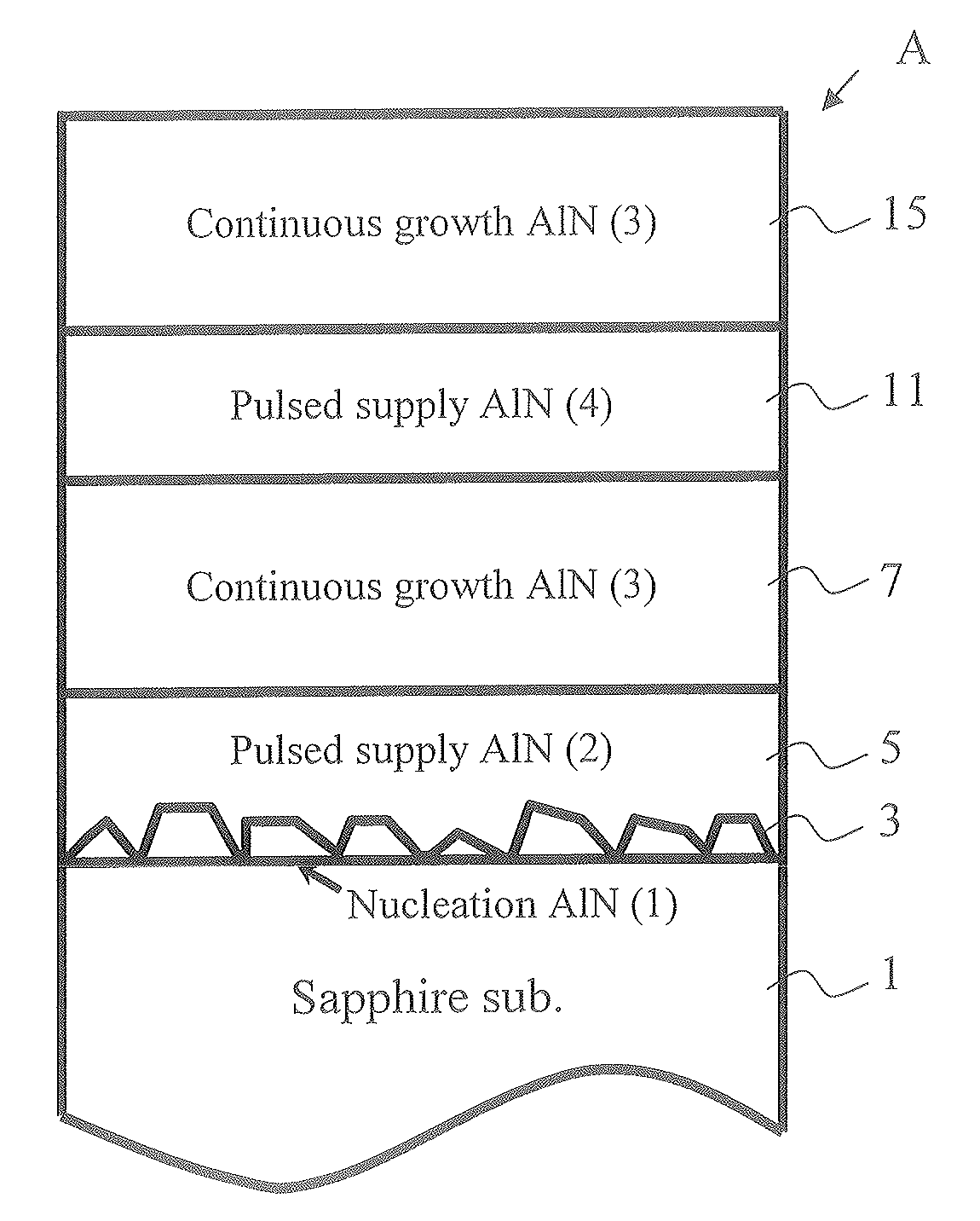
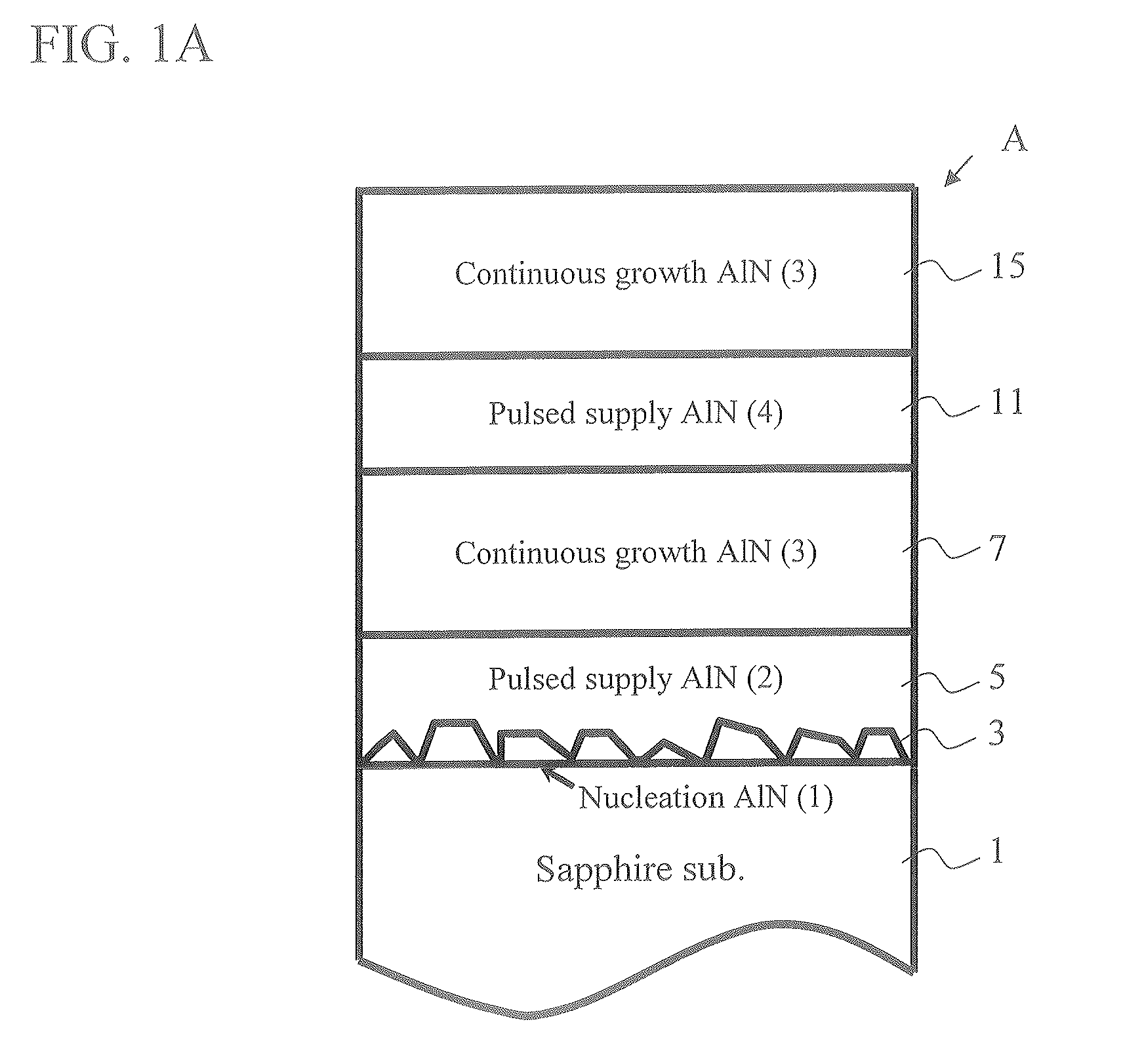
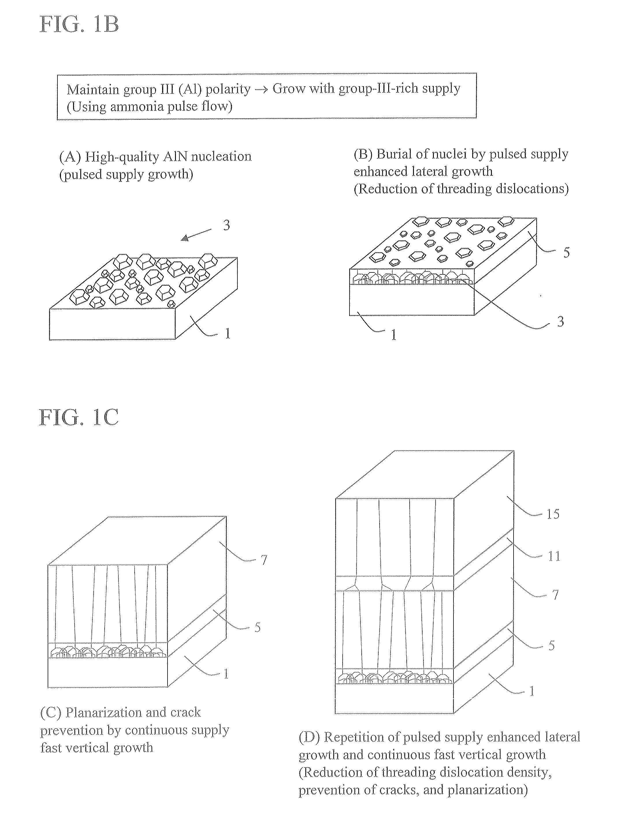
[0045]A principle of an N source pulsed supply multi-step growth technique according to an embodiment of the present invention will be described below. FIG. 1A shows an exemplary AlN high-quality buffer growth structure on a sapphire substrate according to the embodiment. FIG. 2 shows exemplary conditions under which an AlN high-quality buffer layer is grown. FIG. 3 is an example of a sequence diagram for AlN growth by NH3 pulsed supply, which is one of the key points of the embodiment. FIGS. 1B and 1C are diagrams of a specific manufacturing process also showing how threading dislocations are reduced.

[0046]As shown in FIG. 1A, an AlN high-quality buffer growth structure A on sapphire according to the embodiment includes a sapphire (0001) substrate 1, an AlN nucleation layer 3 formed on the sapphire substrate 1, a pulsed supplied AlN layer 5 formed on the AlN nucleation layer 3, and a continuous growth AlN layer 7 formed on the pulsed supplied AlN layer 5. Formed on the continuous g...


PUM


Abstract

Because of a large lattice mismatch between a sapphire substrate and a group III-V compound semiconductor, a good crystal is difficult to grow. A high-quality AlN buffer growth structure A on a sapphire substrate includes a sapphire (0001) substrate 1, an AlN nucleation layer 3 formed on the sapphire substrate 1, a pulsed supplied AlN layer 5 formed on the AlN nucleation layer 3, and a continuous growth AlN layer 7 formed on the pulsed supplied AlN layer 5. Formed on the continuous growth AlN layer 7 is at least one set of a pulsed supplied AlN layer 11 and a continuous growth AlN layer 15. The AlN layer 3 is grown in an initial nucleation mode which is a first growth mode by using an NH3 pulsed supply method. The pulsed supplied AlN layer 5 is formed by using NH3 pulsed supply in a low growth mode which is a second growth mode that increases a grain size and reduces dislocations and therefore is capable of reducing dislocations and burying the nucleation layer 3. The continuous growth AlN layer 7 is a fast vertical growth mode that improves flatness and suppresses crack occurrences. As examples of the thickness of layers; the pulsed supplied AlN layer 5, 11 is 0.3 μm and the thickness of the continuous growth AlN layer 7, 15 is 1 μm, for example. Characteristics of conditions under which layers are grown are as follows. The AlN layer 3 is grown under a high temperature and a high pressure with a low V-III ratio (less N). The pulsed supplied AlN layer 5 is grown at a low temperature and a low pressure with a high V-III ratio (more N). The continuous AlN layer 7 is grown at a high temperature and a high pressure with a high V-III ratio (Al rich and less N) without using an NH3 pulsed supply AlN growth method.

Description

BACKGROUND OF THE INVENTION[0001]1. Field of the Invention[0002]The present invention relates to an optical semiconductor device and a method for manufacturing the same and, in particular, to a deep ultraviolet light emitting device technology using a group III-V compound semiconductor.[0003]2. Background Art[0004]Nitride semiconductor materials containing nitrogen as a group V element are in the spotlight in the field of semiconductor light emitting devices such as light emitting diodes and laser diodes that use a pn junction, and are being researched and developed. Nitride semiconductors such as AlN, GaN, and InN are direct transition semiconductors and ternary and quaternary mixed crystals have the characteristic of being able to emit light in the range from infrared to deep ultraviolet by setting compositions as appropriate to change band-gaps.[0005]Attention is being paid to semiconductor light emitting devices that use an AlGaInN quaternary mixed crystal as a material of a lig...

Claims


Application Information

Patent Timeline
IPC IPC(8): H01L33/00H01L21/205H01L33/06H01L33/12H01L33/32
CPCH01L21/0237H01L21/0242H01L21/02458H01L33/12H01L21/0254H01L21/0262H01L33/007H01L21/02505
Inventor HIRAYAMA, HIDEKIOHASHI, TOMOAKIKAMATA, NORIHIKO
Owner RIKEN
Why Eureka
Try Eureka