Photolithographic mask exhibiting enhanced light transmission due to utilizing sub-wavelength aperture arrays for imaging patterns in nano-lithography

a technology of nano-lithography and sub-wavelength aperture array, which is applied in the field of photolithography, can solve the problems of requiring a lengthy writing process, and achieve the effect of improving light transmission

Active Publication Date: 2009-03-12
UNIV OF MARYLAND
View PDF0 Cites 4 Cited by
  • Summary
  • Abstract
  • Description
  • Claims
  • Application Information

AI Technical Summary

Benefits of technology

[0014]It is therefore an object of the present invention to provide a photolithographic mask exhibiting enhanced light transmission due to the plasmonic excitation of the incident light in sub-wavelength apertures formed in an array formed in the mask to collect and re-radiate optical energy suitable for imaging nano patterns in ultra-high resolution photolithographic printing.

Problems solved by technology

The necessity to expose all pixels of the opaque mask plate corresponding to the clear region requires a lengthy writing process for the conventional mask.

Method used


Image

  • Photolithographic mask exhibiting enhanced light transmission due to utilizing sub-wavelength aperture arrays for imaging patterns in nano-lithography
  • Photolithographic mask exhibiting enhanced light transmission due to utilizing sub-wavelength aperture arrays for imaging patterns in nano-lithography
  • Photolithographic mask exhibiting enhanced light transmission due to utilizing sub-wavelength aperture arrays for imaging patterns in nano-lithography

Examples


Embodiment Construction

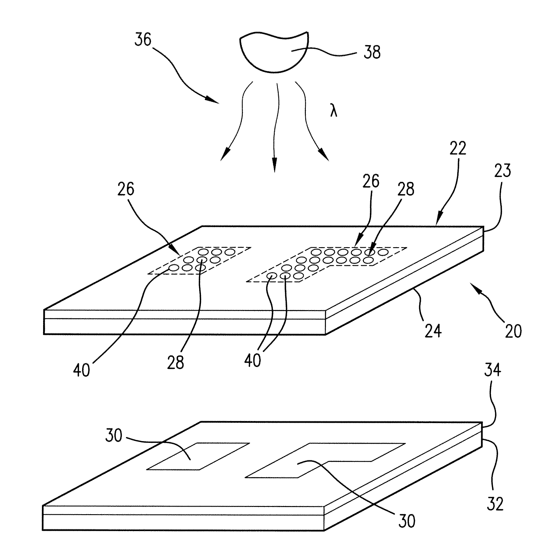
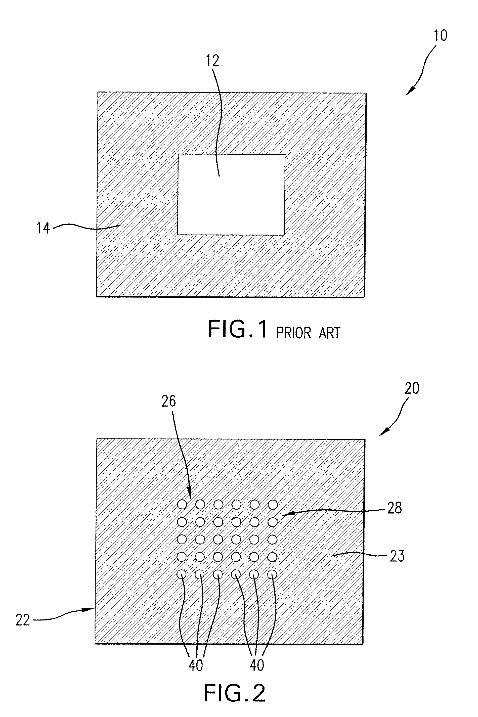
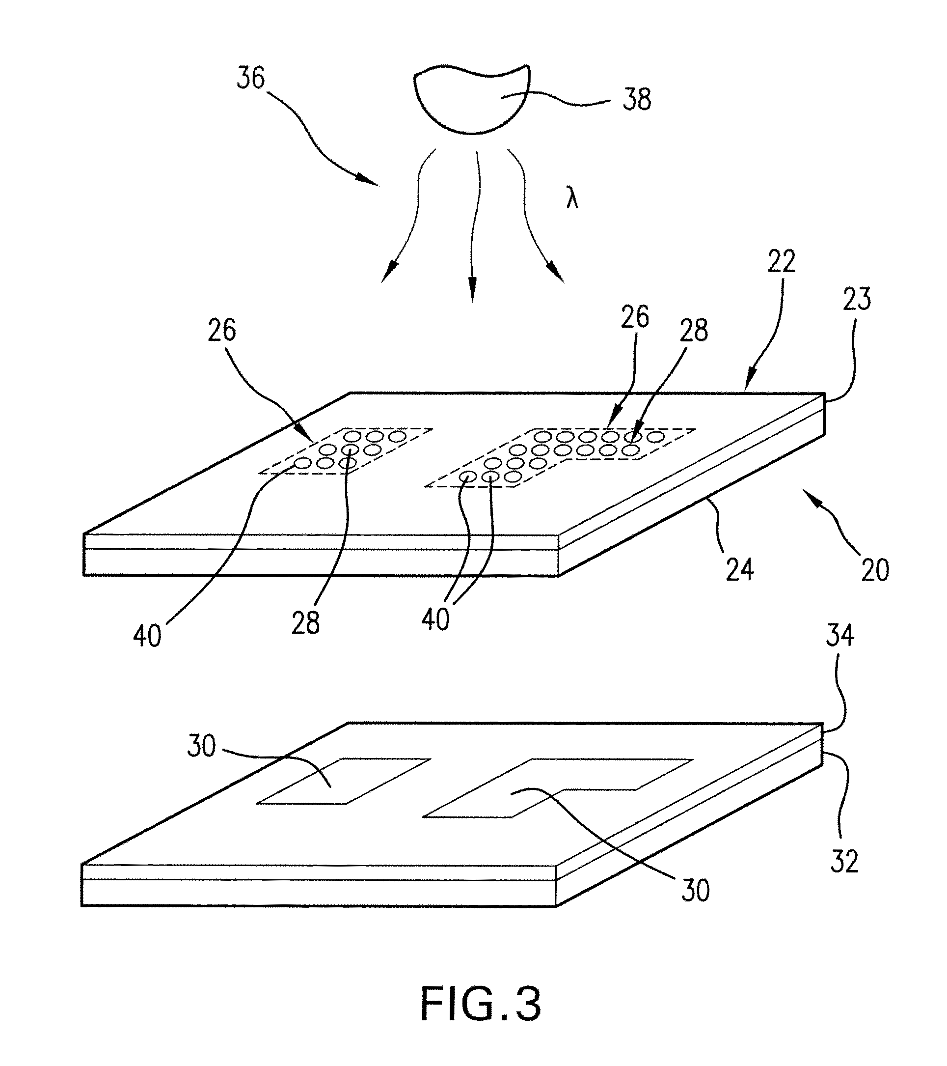
[0042]Referring to FIGS. 2 and 3, mask 20 includes a mask plate (also referred to herein as a photo-plate) 22 formed as a layer 23 of an electrically conducting and optically opaque material, such as, for example, Ag, Al, or Cr, deposited on a mask substrate 24 fabricated from an optically transparent material, such as, for example, glass, quartz, etc. The layer 23 is preferably a thin layer having a predetermined thickness which can be milled through, for example, by a Focused Ion Beam (FIB), as will be described in further paragraphs, during an appropriate exposure time. As an example, the thickness of the opaque layer 23 may be chosen in the range of 100 nm. As shown in FIGS. 2 and 3, the mask 20 may be formed with a single or a plurality of pattern areas 26 in each of which an aperture array 28 is formed.

[0043]The layout of the mask 20, e.g. the number and the shape of pattern areas 26, location thereof on the mask plate 22, spacing therebetween, shape of the aperture array ther...


PUM

PropertyMeasurementUnit
thicknessaaaaaaaaaa
thickaaaaaaaaaa
melting pointaaaaaaaaaa

Abstract

A nanophotolithography mask includes a layer of an electrically conductive optically opaque material deposited on a mask substrate in which regular arrays of sub-wavelength apertures are formed. The plasmonic excitation in the layer perforated with the sub-wavelength apertures arrays under the light incident on the mask produces high resolution far-field radiation patterns of sufficient intensity to expose a photoresist on a wafer when propagated to the same. The fill-factor of the mask, i.e., the ratio of the total apertures area to the total mask area, may lead to a significant increase in mask manufacturing throughput by FIB or electron beam “writing”. The mask demonstrates the defect resiliency and ability to imprint coherent clear features of nano dimensions and shapes on the wafers for integrated circuits design.

Description

[0001]This utility Patent Application is based on the Provisional Patent Application Ser. No. 60 / 924,179 filed 2 May 2007.STATEMENT REGARDING FEDERALLY SPONSORED RESEARCH OR DEVELOPMENT[0002]The development of the invention described herein was funded by the U.S. Naval and Air Systems Command (NAVAIR) under Grant Number N004210310002. The U.S. Government has certain rights in this invention.FIELD OF THE INVENTION[0003]The present invention relates to photolithography, and in particular to an ultra-high resolution nano-lithographic system for “imprinting” nano-sized features on a substrate (wafer).[0004]More in particular, the present invention is directed to a photolithographic mask for use in a nano-lithographic process for imaging patterns on wafers.[0005]In overall concept, the present invention relates to a photolithographic mask exhibiting enhanced light transmission due to plasmonic excitation of the incident light in a sub-wavelength aperture array formed in a metal film of t...

Claims


Application Information

Patent Timeline
Patent Type & Authority Applications(United States)
IPC IPC(8): G03F1/00B29C35/02
CPCG03F1/54G03F1/14G03F7/70433G03F1/50
Inventor PECKERAR, MARTIN C.DAGENAIS, MARIODUTT, BIRENDRABARRY, JOHN D.MESSINA, JR., MICHAEL D.NGU, YVES
Owner UNIV OF MARYLAND
Why Eureka
Try Eureka