
Patterned inorganic LED device

a technology of led devices and inorganic light, which is applied in the manufacture of electrode systems, cold cathode manufacturing, and electric discharge tubes/lamps, etc., can solve the problems of thermal coefficient of expansion mismatch between the shadow mask and the thermal coefficient of expansion, and the difficulty of large substrates

Inactive Publication Date: 2009-03-12
NANOCO TECH LTD
View PDF15 Cites 5 Cited by
  • Summary
  • Abstract
  • Description
  • Claims
  • Application Information

AI Technical Summary

Benefits of technology

This approach improves light emission efficiency, reduces manufacturing complexity, and increases the aperture ratio, leading to higher brightness and longer lifetimes for LED displays while maintaining environmental stability.

Problems solved by technology

One of the main challenges of manufacturing full-color displays is the patterning of light-emissive materials.
Although shadow mask deposition of organic LED materials can work on a substrate of moderate size, e.g., 300 mm×400 mm, it becomes difficult with larger substrates or when the pixel density becomes very high, such as in top-emitting displays.
One problem is the handling (fabrication, alignment, etc.) of such large, thin, and fragile shadow masks.
Another problem is the thermal coefficient of expansion mismatch between the shadow mask, through which the organic LEDs are deposited, and the underlying substrate.
This leads to misalignment of the mask and the proper deposition area on the substrate.
Furthermore, this technique is not useful for patterning materials that are not readily evaporated.
Another challenge to top-emitting LED devices is that a transmissive top electrode is typically provided as a common electrode for many or all pixels.
Unfortunately, the most effective transmissive electrode materials, e.g., ITO and other metal oxides, have insufficient conductivity across the substrate, especially for large substrates.
Numerous bussing designs have been proposed, e.g., in U.S. Published Patent Application Nos. 2004 / 0253756; 2002 / 0011783 and 2002 / 0158835, but such designs add additional complexity to the manufacturing process.
The dominant ones have high manufacturing costs; difficulty in combining multi-color output from the same chip; efficiency of light output; and the need for high-cost rigid substrates.
Because of problems such as aggregation of the quantum dots in the emitter layer, the efficiency of these devices was rather low in comparison with typical OLED devices.
The efficiency was even poorer when a neat film of quantum dots was used as the emitter layer (Hikmet et al., Journal of Applied Physics 93, 3509-3514 (2003)).
The poor efficiency was attributed to the insulating nature of the quantum dot layer.
The resulting device had a poor external quantum efficiency of 0.001 to 0.01%.
These organic ligands are insulators and would result in poor electron and hole injection onto the quantum dots.
In addition, the remainder of the structure is costly to manufacture, due to the usage of electron and hole semiconducting layers grown by high-vacuum techniques, and the usage of sapphire substrates.
In general, bottom-emitting LED devices are easier to manufacture, because the transparent electrode (e.g. ITO) employed in a top-emitting device may be difficult to deposit over the charge-control and light-emitting layers without damaging them and suffers from limited conductivity.
However, active-matrix bottom-emitting LED devices suffer from a reduced light-emitting area (aperture ratio), since a significant proportion (over 70%) of the substrate area can be taken up by the active-matrix components, bus lines, etc.
Since some LED materials degrade in proportion to the current density passed through them, a reduced aperture ratio will increase the current density through the layers at a constant brightness, thereby significantly reducing the LED device's lifetime.
Thin-film, LED devices in general suffer from a loss of light trapped in various layers of the LED, substrate, or cover, thereby decreasing the efficiency of the LED device.
Hence, light emitted in a layer at a high angle with respect to the substrate normal can internally reflect and become trapped in the high optical-index materials of the layers and transparent electrodes; thereby reducing the efficiency of the LED device.
However, scattered light can propagate a considerable distance horizontally through the cover, substrate, or organic layers before being scattered out of the device, thereby reducing the sharpness of the device in pixelated applications such as displays.

Method used


Image

  • Patterned inorganic LED device
  • Patterned inorganic LED device
  • Patterned inorganic LED device

Examples


Embodiment Construction

[0030]A color LED display emits light of at least one color. The term “multicolor” is employed to describe a display panel that is capable of emitting light of different hues in different areas. In particular, “multicolor” is employed to describe a display panel that is capable of displaying images of different colors. These areas are not necessarily contiguous. The term “full color” is employed to describe multicolor display panels that are capable of emitting in several regions of the visible spectrum and therefore displaying images in a large combination of hues. The red, green, and blue colors constitute the three primary colors from which all other colors can be generated by appropriate mixing. However, for this invention, “full-color” can include additional different colored pixels. The term “hue” refers to the intensity profile of light emission within the visible spectrum, with different hues exhibiting visually discernible differences in color. The term “pixel” designates a...


PUM

PropertyMeasurementUnit
sizeaaaaaaaaaa
external quantum efficiencyaaaaaaaaaa
refractive indexaaaaaaaaaa

Abstract

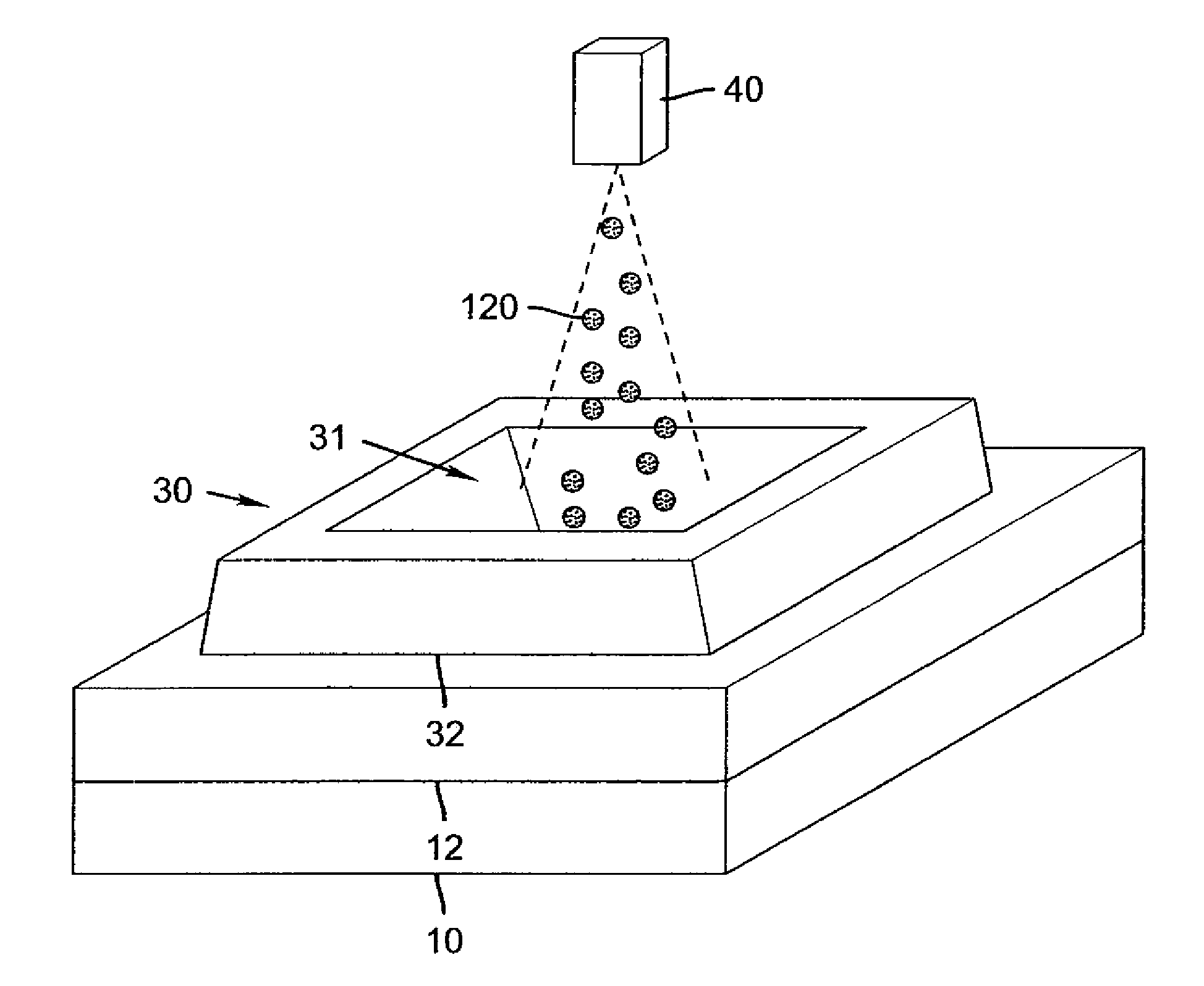
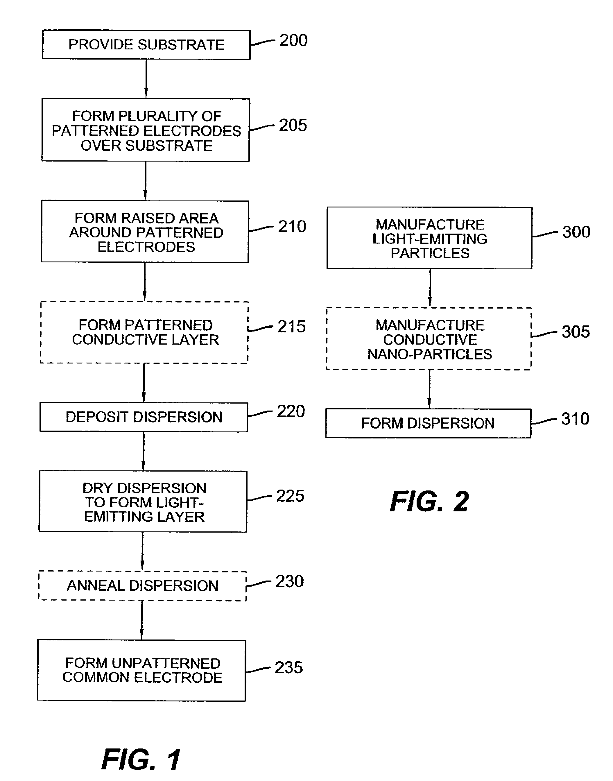
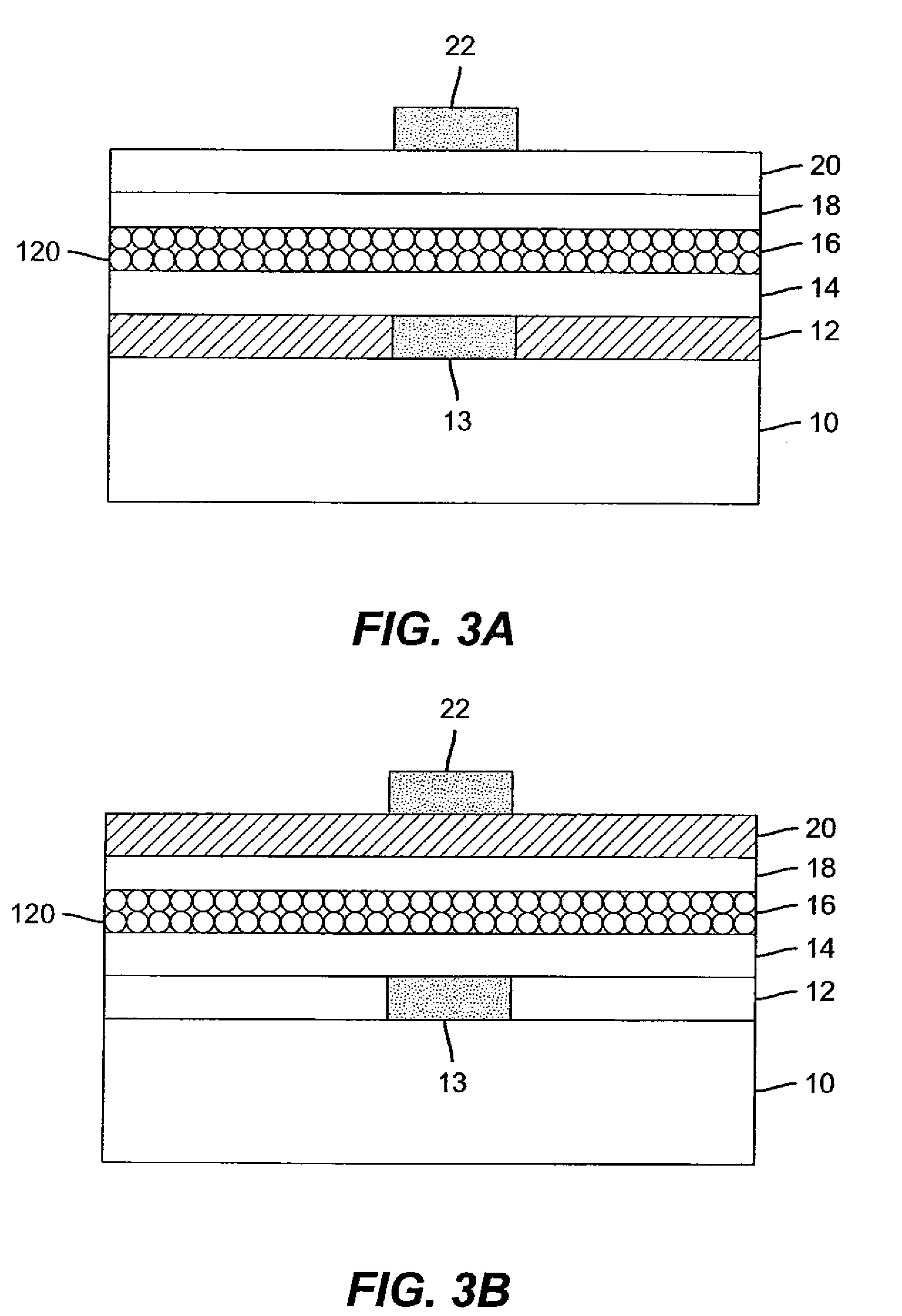
A method of making an inorganic light-emitting diode display having a plurality of light-emitting elements including providing a substrate, and forming a plurality of patterned electrodes over the substrate. A raised area is formed around each patterned electrode to provide a well before depositing a dispersion containing inorganic, light-emissive core / shell nano-particles into each well. The dispersion is dried to form a light-emitting layer including the inorganic, light-emissive core / shell nano-particles. An unpatterned, common electrode is formed over the light-emitting layer. The light-emitting layer emits light by the recombination of holes and electrons supplied by the electrodes.

Description

CROSS REFERENCE TO RELATED APPLICATION[0001]This application is a divisional of commonly assigned U.S. patent application Ser. No. 11 / 681,920 filed Mar. 5, 2007, the disclosure of which is incorporated herein.FIELD OF THE INVENTION[0002]The present invention relates to inorganic light emitting diode (LED) displays having a plurality of pixels, and more particularly, to inorganic displays having improved emitter patterning, light efficiency, and transparent electrode conductivity.BACKGROUND OF THE INVENTION[0003]Flat-panel displays, such as light emitting diode (LED) displays, of various sizes are proposed for use in many computing and communication applications. In its simplest form, an LED includes an anode for hole injection, a cathode for electron injection, and a light-emitting medium sandwiched between these electrodes to support charge recombination that yields emission of light. LED displays can be constructed to emit light through a transparent substrate (commonly referred t...

Claims


Application Information

Patent Timeline
Patent Type & Authority Applications(United States)
IPC IPC(8): H01J9/12
CPCH05B33/145
Inventor COK, RONALD S.
Owner NANOCO TECH LTD
Learn More