

(Al,In,Ga,B)N DEVICE STRUCTURES ON A PATTERNED SUBSTRATE
a technology of patterned substrates and device structures, which is applied in the direction of semiconductor/solid-state device manufacturing, semiconductor devices, electrical devices, etc., can solve the problems of affecting the extraction efficiency of nitride-based devices grown on sapphire, affecting the efficiency of nitride-based devices, and affecting the propagation of most of the light generated, so as to improve the electronic efficiency characteristics of nitride-based device structures, improve the light emission efficiency, and enhance the output power
- Summary
- Abstract
- Description
- Claims
- Application Information
AI Technical Summary
Benefits of technology
Problems solved by technology
Method used
Image

Examples
embodiment 1
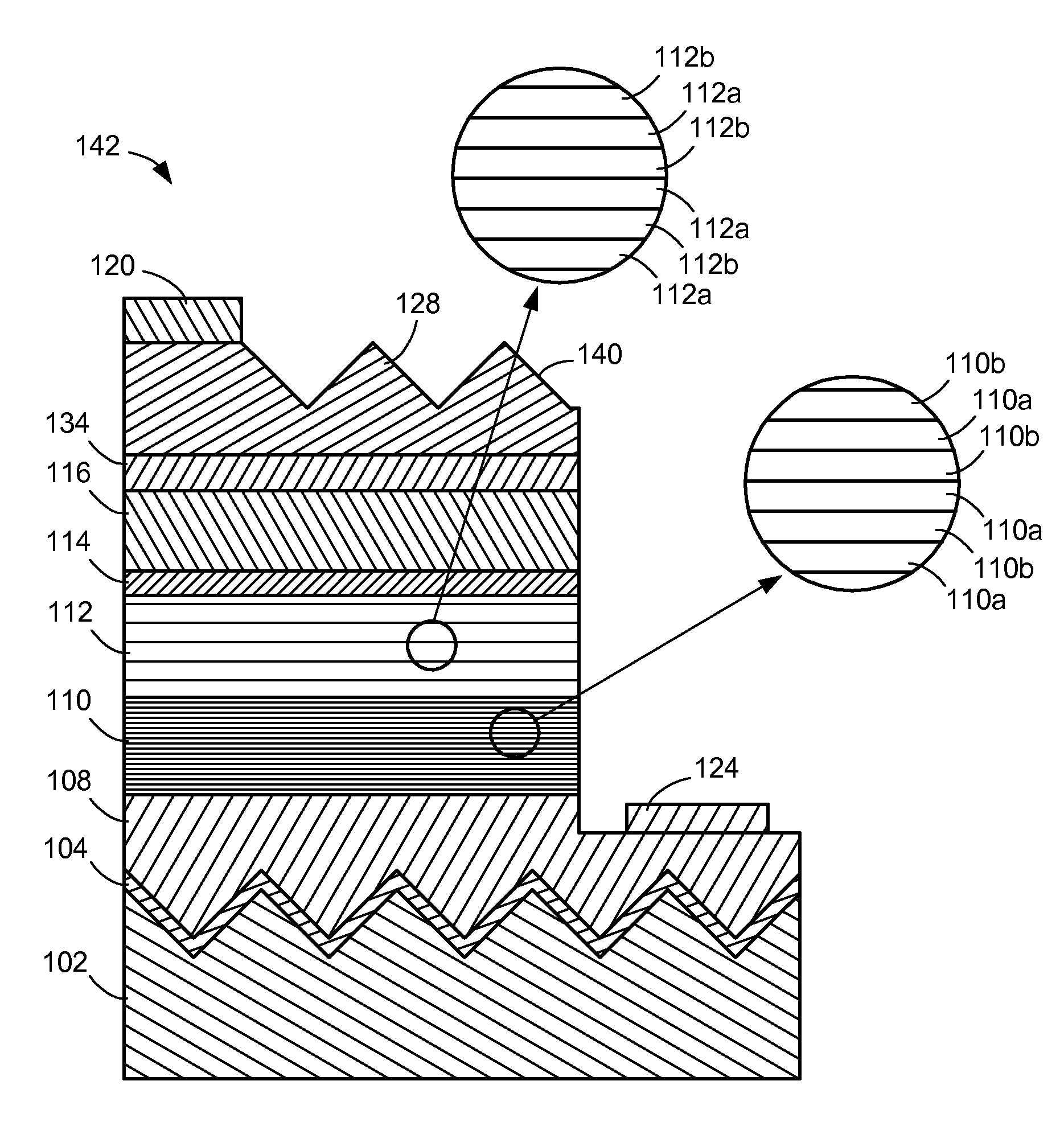
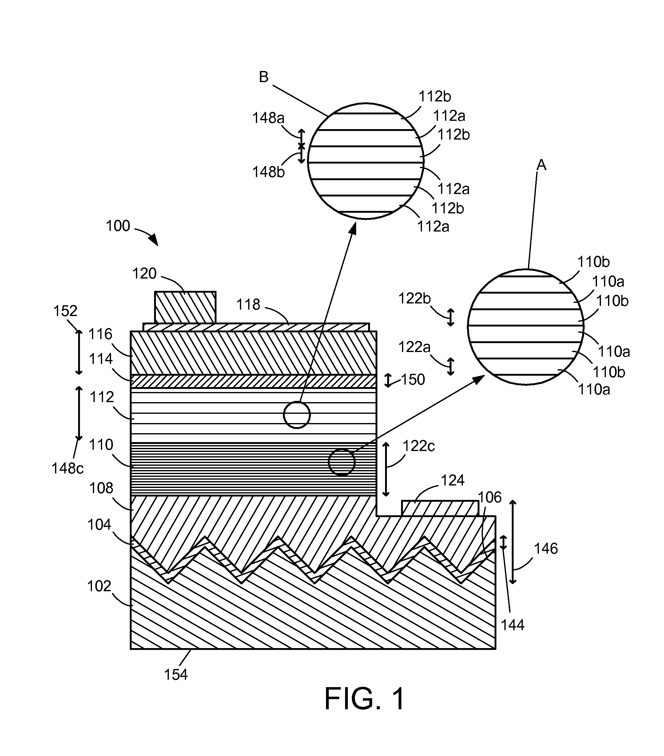
[0063]FIG. 1 is a schematic sectional view showing the structure of a nitride semiconductor device (an LED device) 100 according to embodiment 1 of the present invention. This LED 100 comprises a patterned sapphire substrate 102, and deposited successively in the following order on the substrate 102: a first buffer layer 104 made of GaN (closest to the substrate 102 surface 106), an n-contact layer 108 made of GaN doped with silicon, an n-side multi-layer film made of an InGaN / GaN superlattice structure 110 (which may comprise layers 110a and 110b), an active layer 112 comprising a multiple quantum well structure made of InGaN / GaN (which may comprise layers 112a and 112b), a p-side AlGaN electron blocking layer 114 doped with magnesium, a p-contact layer 116 comprising GaN doped with magnesium, a thin transparent p-contact layer 118, and a thick p-pad layer 120 that is the furthest from the substrate 102 patterned surface 106.
[0064]The LED device 100 has the active layer 112 of the ...
embodiment 2
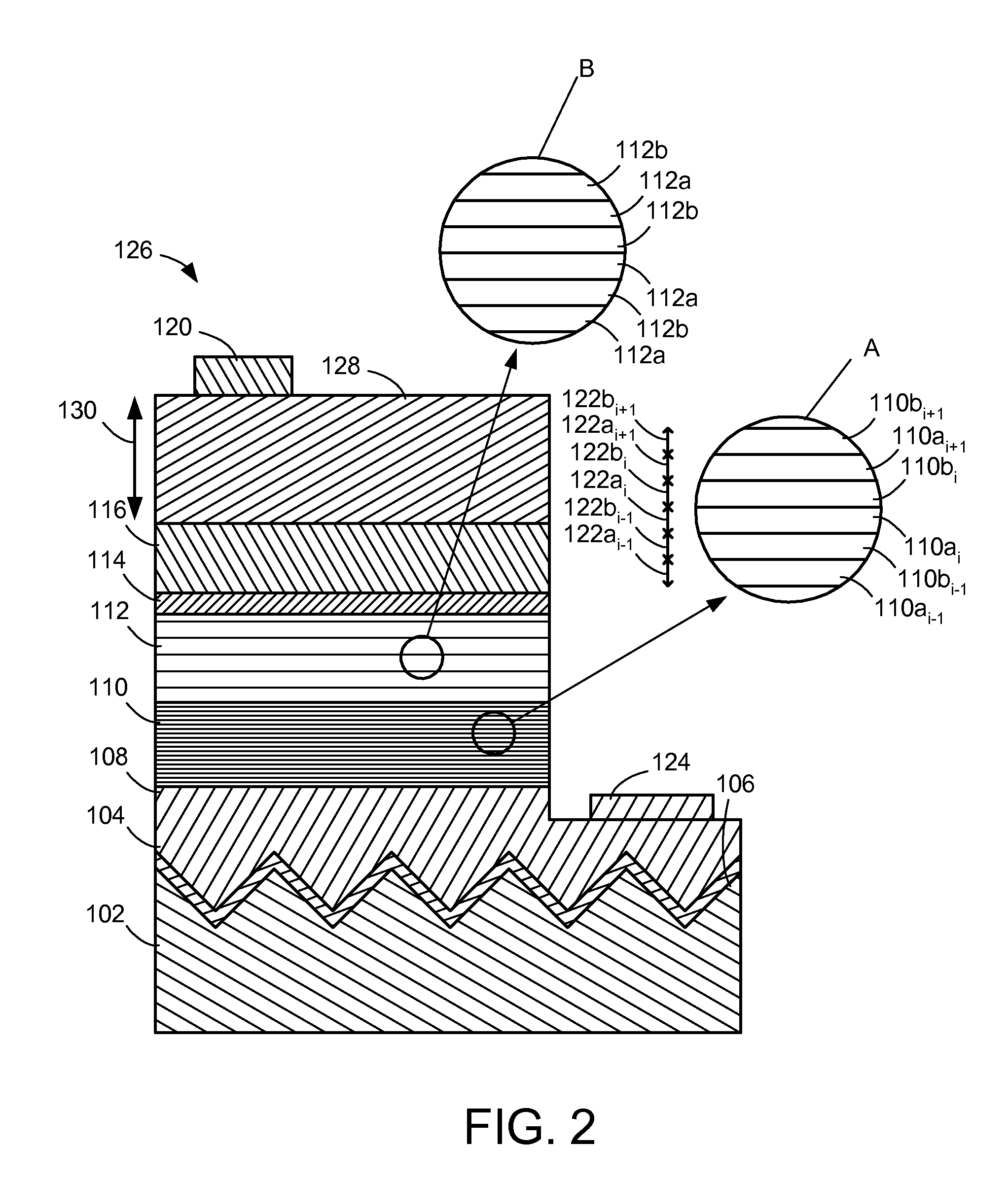
[0079]The nitride semiconductor light emitting device 126 according to embodiment 2, as shown in FIG. 2, has the same structure as in embodiment 1, except that the transparent p-contact layer 128 in embodiment 2 is comprised of a novel p-contact such as a TCO, thereby substituting the thin semi-transparent p-electrode layer 118 described in embodiment 1.
[0080]Specifically, the TCO 128 may be comprised of elements such as ZnO or ITO.
[0081]These layers 128 can be deposited in-situ, such as in an MOCVD reactor, or can be subsequently laminated in a separate deposition process. The TCO 128 can also be structurally bonded using an appropriate process.
[0082]Also, the TCO film or films 128 may comprise a plurality of different layers and compositions. They can also be unintentionally doped or intentionally doped with various elements in order to tailor the films' 128 properties, such as electrical conductivity and structural composition. The TCO layer 128 may be used as a p-type contact to...
embodiment 3
[0084]The nitride semiconductor light emitting diode 132 according to embodiment 3, as shown in FIG. 3, has the same structure as embodiment 2, except that a tunnel junction layer 134 is laminated between the p-type GaN contact layer 116 and the TCO 128.
[0085]The tunnel junction layer 134 may be comprised of a nitride semiconductor which is intentionally doped with an n-type or p-type impurity, such as elements of silicon or magnesium, in order to control the conductivity of the layer 134. The tunnel junction layer 134 can be comprised of various thicknesses 136 and compositions. It 134 can also be comprised of a plurality of different layers. It 134 can also be doped with graded compositions or modulation doped.
[0086]For example, the tunnel junction layer 134 may be a nitride-based layer, comprising GaN, for example, or the tunnel junction layer may contains at least some indium.
PUM
| Property | Measurement | Unit |
|---|---|---|
| composition | aaaaa | aaaaa |
| thickness | aaaaa | aaaaa |
| critical elastic thickness | aaaaa | aaaaa |
Abstract
Description
Claims
Application Information