Gallium nitride bulk crystals and their growth method
a technology of gallium nitride and bulk crystals, which is applied in the direction of crystal growth process, polycrystalline material growth, chemistry apparatus and processes, etc., can solve the problems of deteriorating the performance and reliability of these devices, difficult to grow a bulk crystal of gan, and existing technology is limited by the crystal siz
- Summary
- Abstract
- Description
- Claims
- Application Information
AI Technical Summary
Benefits of technology
Problems solved by technology
Method used
Image
Examples
example 1
Run Number THV2008(Not Using an Internal Chamber)
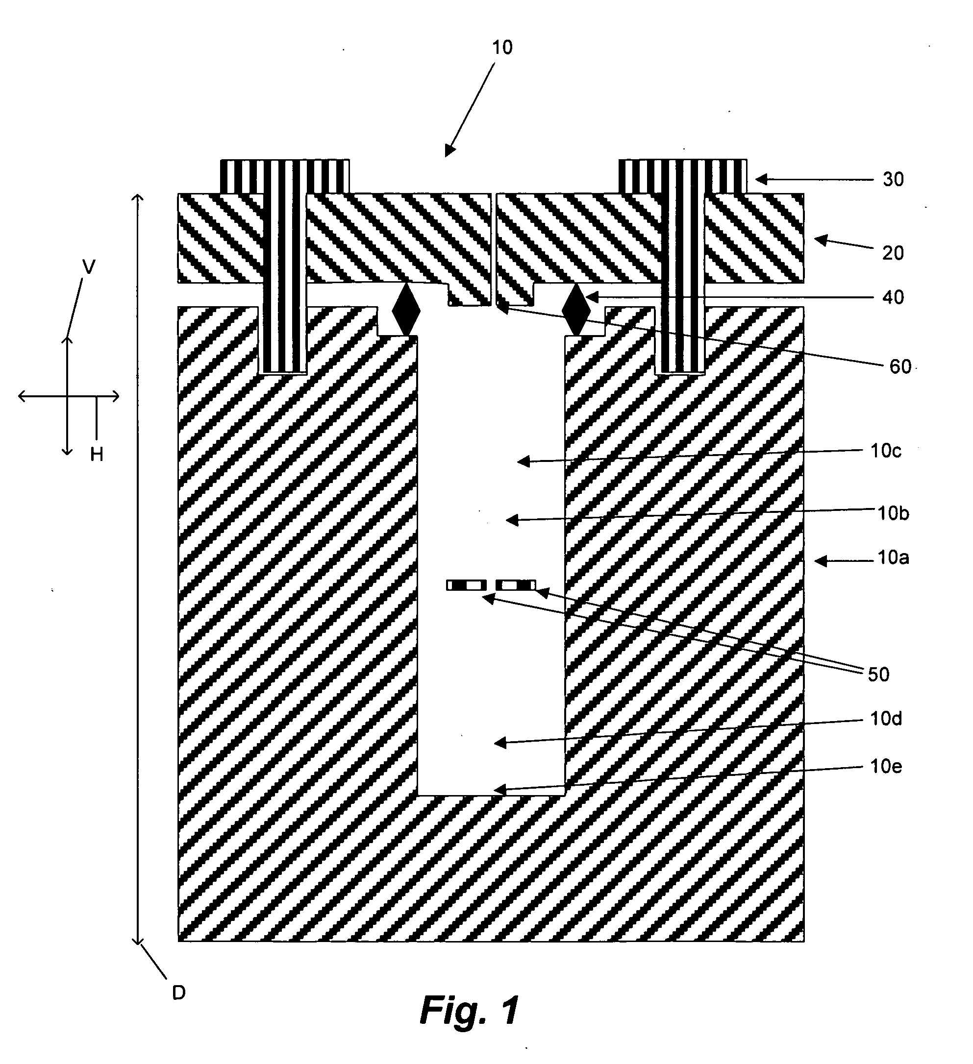
[0049]In this example, GaN was grown in a high-pressure vessel comprising an autoclave having an inner diameter of 1 inch, inner height of 10 inches and three baffle plates at the middle height of the chamber. First, 4.377 g of NaNH2 was loaded at the bottom of the autoclave. Then, platelet-shaped c-plane GaN seed crystals (one in a rectangular shape having a longest dimension of about 4.5 mm, and the other in a triangular shape having a longest dimension of about 6 mm) were loaded in the lower region of the autoclave and 30 g of polycrystalline GaN, contained in a Ni—Cr mesh basket, was loaded in the upper region of the autoclave. These solid sources were loaded in a glove box in which the oxygen and moisture concentration is controlled to be less than 1 ppm. After the lid of the autoclave was tightened, 45.7 g of anhydrous liquid ammonia were condensed in the autoclave. The autoclave was heated by the external heater. The lower regi...
example 2
Run Number C119(Using an Internal Chamber)
[0051]In this example, GaN was grown in a high-pressure vessel comprising an autoclave having an internal chamber. The internal chamber has an inner diameter of 2 inch, an inner height of 10 inches, and three baffle plates at the middle height of the chamber. First, 9.021 g of NaNH2 was loaded at the bottom of the internal chamber. Then, hexagonal rod-shaped GaN seed crystal (with m-plane exposed, approximately 2 mm of point-to-point dimension for the bottom surface and approximately 3 mm in height) was loaded in the lower region of the internal chamber and 100.7 g of polycrystalline GaN, contained in Ni—Cr mesh basket, was loaded in the upper region of the internal chamber. These solid sources were loaded in a glove box in which the oxygen and moisture concentration was controlled to be less than 1 ppm. After the lid of the internal chamber was tightened, 101.5 g of anhydrous liquid ammonia were condensed in the internal chamber. Then the i...
example 3
Wafers Sliced from THV2008
[0053]In this example, the grown GaN boules 250 and 260 shown in FIGS. 5(a) and 6(a) were sliced with a wire saw. The dimension of the grid in FIG. 5(a) and 6(a) is 1 mm. FIG. 5(b), FIG. 5(c), FIG. 5(d), and FIG. 5(e) show c-plane wafers and FIG. 6(b), FIG. 6(c), FIG. 6(d), FIG. 6(e), FIG. 6(f), FIG. 6(g), and FIG. 6(h) show m-plane wafers. This example demonstrates the ease of fabricating wafers with any favorable orientations.
[0054]In FIG. 5(a), the parallel lines 270 represent approximate wire saw positions to cut the slices shown in FIG. 5(b), FIG. 5(c), FIG. 5(d), and FIG. 5(e), wherein the slices of FIG. 5(b), FIG. 5(c), FIG. 5(d), and FIG. 5(e) correspond to the ordering of parallel lines 270 from top to bottom. The rectangle 280 in FIG. 5(a) shows the position of the seed crystal for the growth of the boule 250.
[0055]In FIG. 6(a), the parallel lines 290 represent approximate wire saw position to cut the slices of FIG. 6(b), FIG. 6(c), FIG. 6(d), FI...
PUM
 Abstract
Description
Claims
Application Information


