Manufacturing method of light emitting device, and evaporation donor substrate

a technology of light emitting devices and donor substrates, which is applied in the field of manufacturing methods of light emitting devices and evaporation donor substrates, can solve the problems of difficult application of the method to a high-definition display device, low deposition accuracy, and large size so as to achieve easy manufacturing of light emitting devices and improve patterning precision. , the effect of excellent properties

Inactive Publication Date: 2009-03-19
SEMICON ENERGY LAB CO LTD
View PDF26 Cites 58 Cited by
  • Summary
  • Abstract
  • Description
  • Claims
  • Application Information

AI Technical Summary

Benefits of technology

[0040]Application of the present invention makes it possible to easily form a layer containing an evaporation material, which is included in a light emitting element, and to easily manufacture a light emitting device including the light emitting element.
[0041]Application of the present invention also makes it possible to form a flat even film. In add...

Problems solved by technology

However, this method does not provide very high deposition accuracy and thus requires that the distance between pixels be designed to be large and the width of a partition (bank) formed of an insulator between pixels be large.
Therefore, application of the method to ...

Method used


Image

  • Manufacturing method of light emitting device, and evaporation donor substrate
  • Manufacturing method of light emitting device, and evaporation donor substrate
  • Manufacturing method of light emitting device, and evaporation donor substrate

Examples


embodiment mode 1

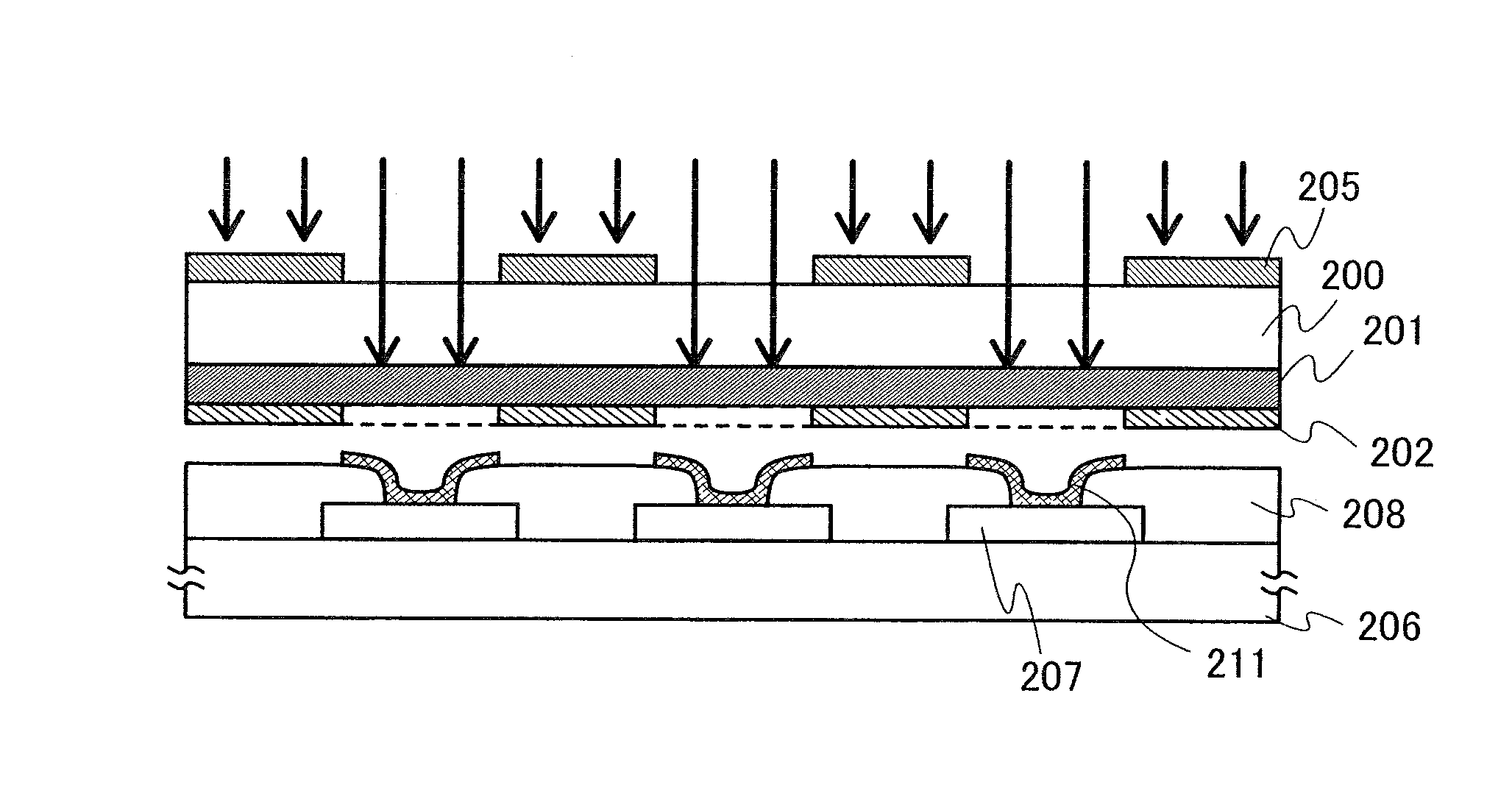
[0067]A manufacturing method of a light emitting device, and an evaporation donor substrate of the present invention are described with reference to FIGS. 1A to 1C.

[0068]FIG. 1A shows an evaporation donor substrate of the present invention. In FIG. 1A, a reflective layer 205 is formed on a first surface side of a first substrate 200 that is a supporting substrate. The reflective layer 205 has an opening. On a second surface side facing the first surface of the first substrate 200, a light absorption layer 201 is formed. In FIGS. 1A to 1C, the light absorption layer 201 is formed over the entire second surface of the first substrate 200. In addition, an evaporation material is attached onto the light absorption layer 201. In FIG. 1A, a first layer 202 containing the evaporation material is formed.

[0069]The first substrate 200 is a supporting substrate for the reflective layer, the light absorption layer, and the like and transmits irradiation light used for evaporating the first laye...

embodiment mode 2

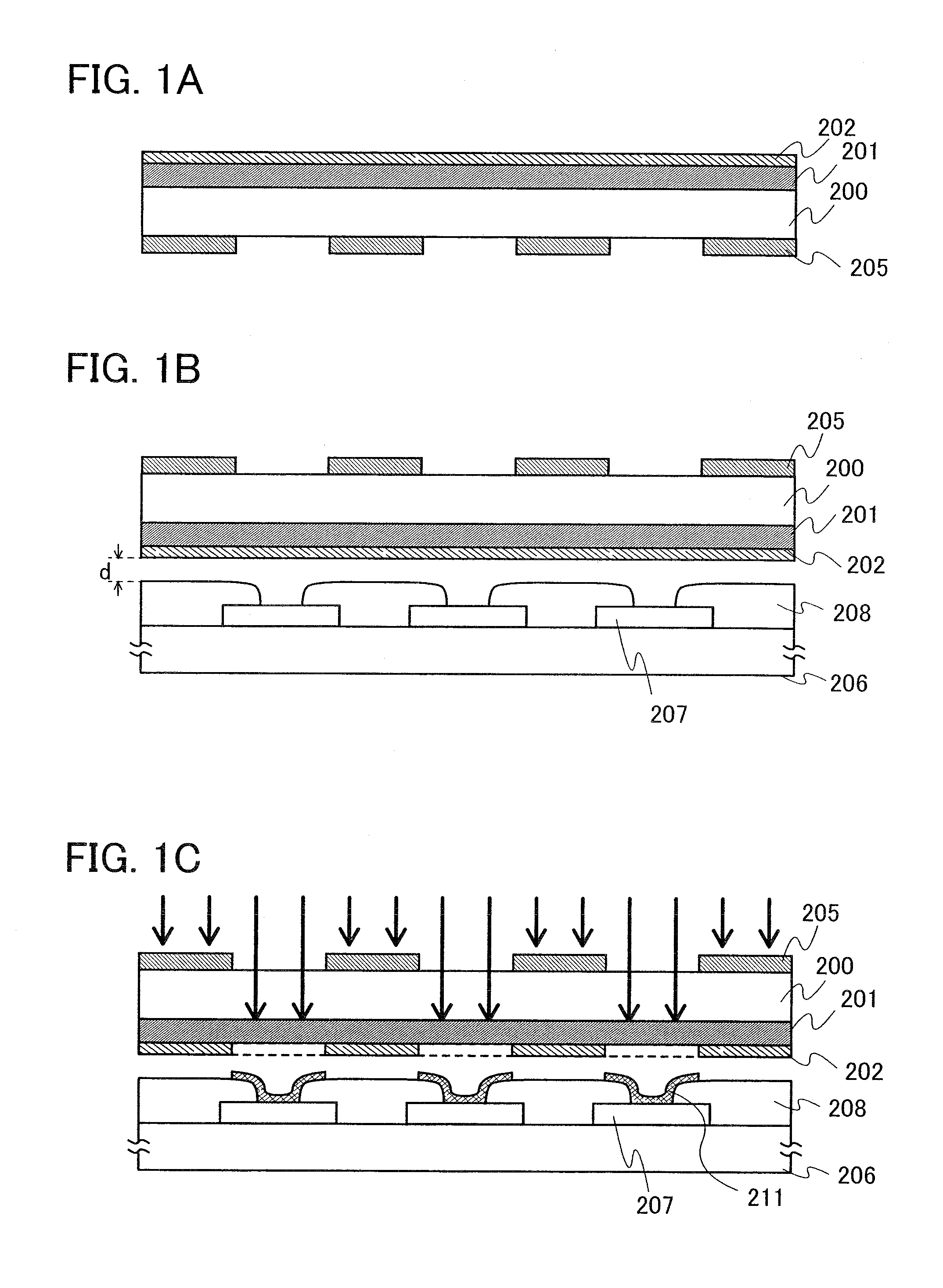
[0107]In this embodiment mode, a manufacturing method of a full-color display device by using the evaporation donor substrate used in Embodiment Mode 1 is described.

[0108]Embodiment Mode 1 shows the example in which deposition is performed onto each of the adjacent first electrode layers 207 in a single deposition step, whereas when a full-color display device is manufactured, light emitting layers which emit light of different colors are formed in different regions through a plurality of deposition steps.

[0109]A manufacturing example of a light emitting device capable of full color display is described below. In this embodiment mode, an example of a light emitting device using light emitting layers which emit light of three colors is described.

[0110]Three evaporation donor substrates each of which is the substrate shown in FIG. 1A are prepared. In each of the evaporation donor substrates, a layer containing a different kind of evaporation material is formed. Specifically, a first e...

embodiment mode 3

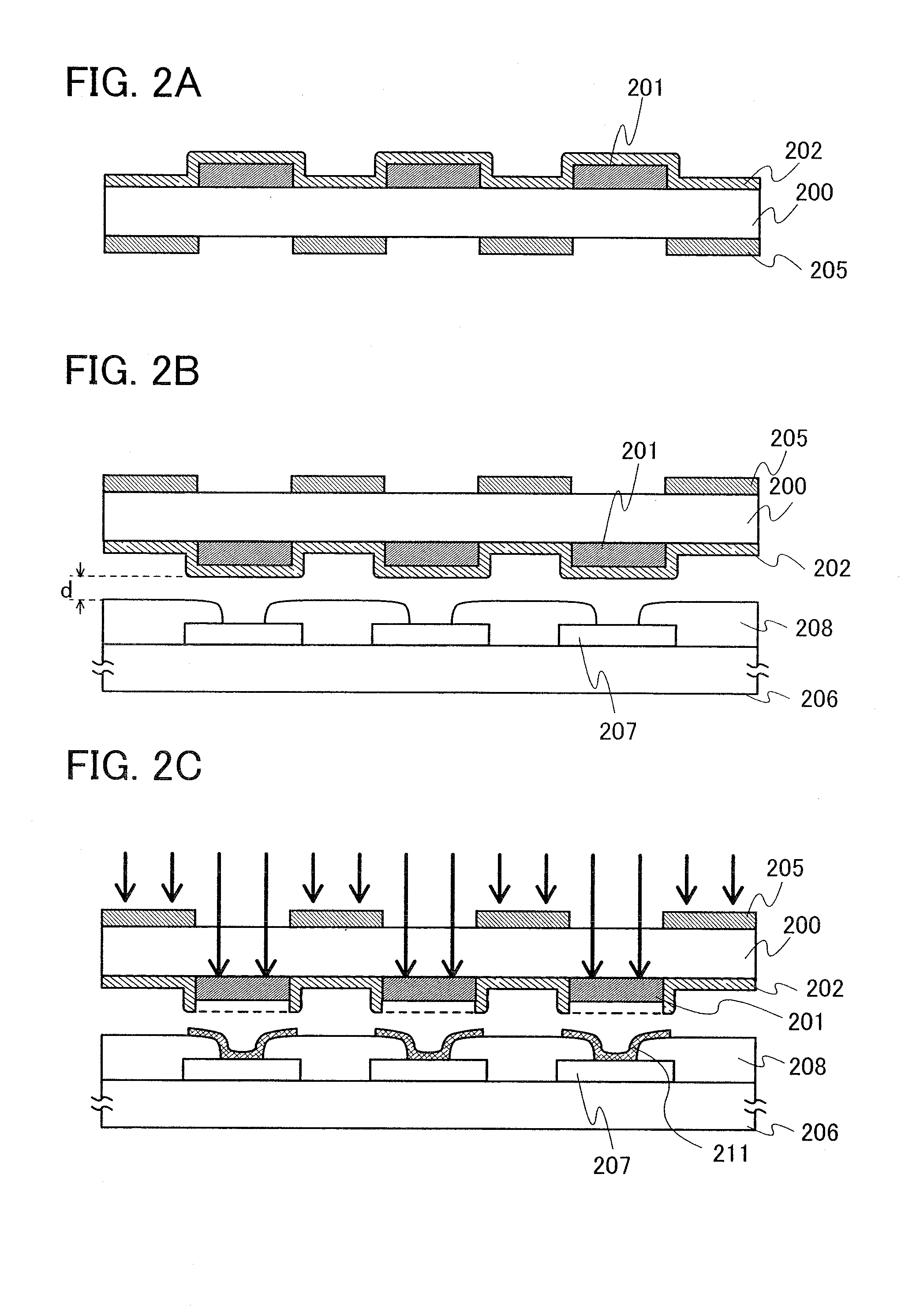
[0126]In this embodiment mode, a manufacturing method of a light emitting element and a light emitting device by application of the present invention is described.

[0127]For example, light emitting elements shown in FIGS. 3A and 3B can be manufactured. In the light emitting element shown in FIG. 3A, a first electrode layer 302, an EL layer 308 which functions as a light emitting layer 304, and a second electrode layer 306 are stacked in this order over a substrate 300. One of the first electrode layer 302 and the second electrode layer 306 functions as an anode, and the other functions as a cathode. Holes injected from an anode and electrons injected from a cathode are recombined in the light emitting layer 304, whereby light emission can be obtained. In this embodiment mode, the first electrode layer 302 functions as the anode and the second electrode layer 306 functions as the cathode.

[0128]In the light emitting element shown in FIG. 3B, in addition to the components shown in FIG. ...


PUM

PropertyMeasurementUnit
Thicknessaaaaaaaaaa
Thicknessaaaaaaaaaa
Reflectanceaaaaaaaaaa

Abstract

An object is to provide a manufacturing method of a light emitting device, by which manufacturing costs in manufacturing a flat panel display can be reduced. A first substrate provided with a reflective layer having an opening over a first surface, and provided with a light absorption layer and an evaporation material over a second surface facing the first surface is used. Then, in a state where the second surface of the first substrate is disposed close to a first surface of a second substrate, light irradiation is performed from the first surface side of the first substrate. The irradiation light is absorbed by a portion of the light absorption layer overlapping with the opening in the reflective layer, thereby heating the evaporation material. The heated evaporation material is attached to the first surface of the second substrate.

Description

BACKGROUND OF THE INVENTION[0001]1. Field of the Invention[0002]The present invention relates to a light emitting device and a manufacturing method of the light emitting device. The present invention also relates to an evaporation donor substrate used for deposition of a material.[0003]2. Description of the Related Art[0004]Organic compounds can take various structures compared with inorganic compounds, and it is possible to synthesize a material having various functions by appropriate molecular design of an organic compound. Owing to these advantages, photo electronics and electronics which employ a functional organic material have been attracting attention in recent years.[0005]A solar cell, a light emitting element, an organic transistor, and the like can be given as examples of electronics devices using an organic compound as a functional organic material. These devices take advantage of electrical properties and optical properties of the organic compound. Among them, in particu...

Claims


Application Information

Patent Timeline
IPC IPC(8): G03F7/00
CPCH01L51/56H01L51/0013C23C14/048H10K71/18H10K71/421H10K71/00
Inventor HIRAKATA, YOSHIHARUIKEDA, HISAOYOKOYAMA, KOHEISATO, YOSUKE
Owner SEMICON ENERGY LAB CO LTD
Why Eureka
Try Eureka