

Gallium nitride-based material and method of manufacturing the same
a technology of gallium nitride and nitride, which is applied in the direction of polycrystalline material growth, crystal growth process, chemically reactive gas growth, etc., can solve the problem of not revealing any practical method, and achieve the effect of high thermal conductivity
- Summary
- Abstract
- Description
- Claims
- Application Information
AI Technical Summary
Benefits of technology
Problems solved by technology
Method used
Image

Examples
example 1
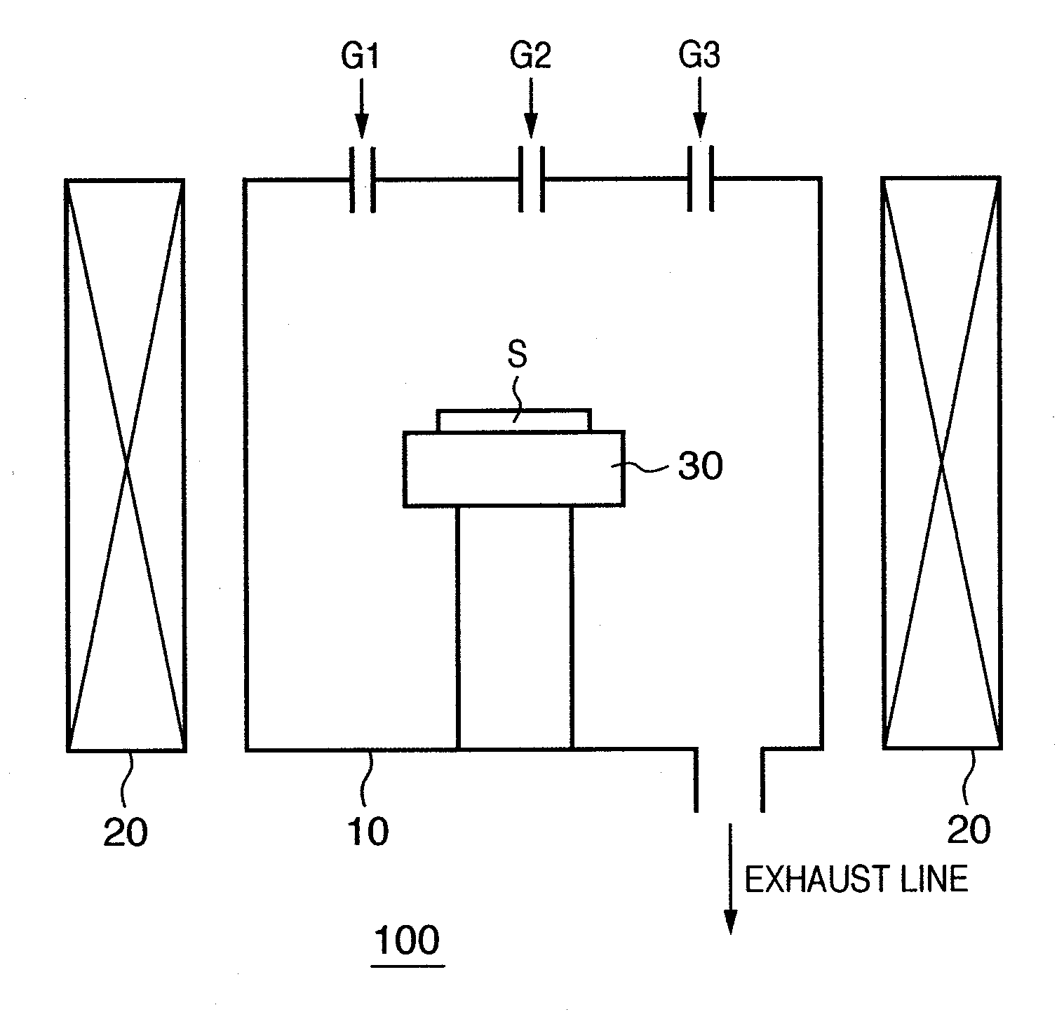
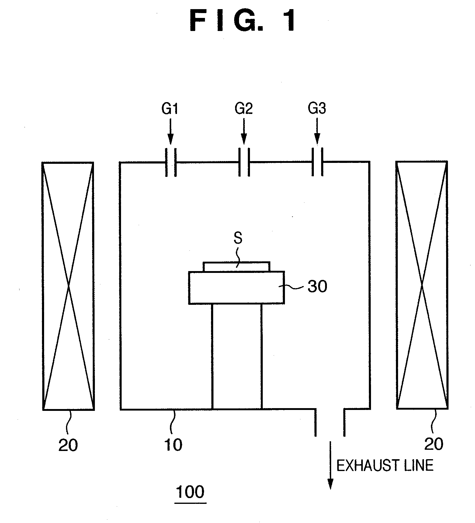
[0113]A sapphire substrate 430 (μm) in thickness and 2 inches in diameter having a (0001) surface was prepared as an underlying substrate, and cleaned with an organic solvent as pre-preprocessing. After that, an underlying GaN layer having a thickness of 2 (μm) was grown on the underlying substrate by using an MOCVD apparatus.
[0114]Subsequently, the substrate having the underlying GaN layer grown on it was placed in the reaction chamber 10 of an HVPE apparatus, and the reaction temperature was raised to 1,070 (° C.). After that, while the carrier gas G1 practically containing only H2, the GaCl gas G2 as the reaction product of Ga and HCl, and the NH3 gas G3 were supplied onto the GaN layer, a GaN layer was grown on the underlying GaN layer for about 15 hrs. In this growth step, the growth pressure was set at 1.01×10⁵ (Pa), the partial pressure of GaCl gas G2 was set at 1.11×10³ (Pa), and the partial pressure of the NH3 gas G3 was set at 4.45×10³ (Pa).
[0115]Then, the sapphire substra...
example 2
[0122]First, a GaN layer was grown on an underlying GaN layer under the same conditions as in Example 1 except that the reaction temperature was set at 1,000 (° C.).
[0123]Then, a sapphire substrate was removed from a substrate on which the GaN layer was grown. In this manner, an Si-doped (the carrier concentration: n-type, 4×10¹⁷ (atoms / cm3), the hole measurement value) self-supporting GaN single-crystal substrate about 1,060 (μm) thick was obtained. The oxygen, carbon, and hydrogen impurity concentrations were respectively less than 2×10¹⁶ (atoms / cm3), 2×10¹⁶ (atoms / cm3), and less than 1×10¹⁷ (atoms / cm3), that is, the oxygen and hydrogen concentrations were less than the detection limits.
[0124]The threading dislocation density measured by CL (Cathode Luminescence) or AEM was 5×10⁶ (dislocations / cm2).
[0125]After that, a square plate-like GaN single-crystal sample of 10 (mm) side having a thickness of 1 (mm) was formed by polishing and shaping the two surfaces of the obtained GaN sin...
example 3
[0129]First, a GaN layer was grown on an underlying GaN layer under the same conditions as in Example 1 except that the reaction temperature was set at 1,100 (° C.).
[0130]Then, a sapphire substrate was removed from a substrate on which the GaN layer was grown. In this way, an Si-doped (the carrier concentration: n-type, 4×10¹⁷ (atoms / cm3), the hole measurement value) self-supporting GaN single-crystal substrate about 1,060 (μm) thick was obtained. The oxygen, carbon, and hydrogen impurity concentrations were respectively less than 2×10¹⁶ (atoms / cm3), less than 1×10¹⁶ (atoms / cm3), and less than 1×10¹⁷ (atoms / cm3), that is, all the impurity concentrations were less than the detection limits.
[0131]The threading dislocation density measured by CL (Cathode Luminescence) or AFM was 3×10⁶ (dislocations / cm2).
[0132]After that, a square plate-like GaN single-crystal sample of 10 (mm) side having a thickness of 1 (mm) was formed by polishing and shaping the two surfaces of the obtained GaN sin...
PUM
 Abstract
Description
Claims
Application Information