Non-polar and semi-polar GaN substrates, devices, and methods for making them

a technology of non-polar and semi-polar gan, which is applied in the direction of crystal growth process, polycrystalline material growth, chemically reactive gas growth, etc., can solve the problems of reducing the recombination efficiency of electron-hole pairs, affecting the performance of nitride-based devices, and piezoelectric polarization

Active Publication Date: 2009-03-26
KYMA TECH
View PDF9 Cites 326 Cited by
  • Summary
  • Abstract
  • Description
  • Claims
  • Application Information

AI Technical Summary

Benefits of technology

[0014]According to another implementation, a method is provided for making a re-grown GaN crystal is provided. A non-polar GaN seed crystal is provided. The non-polar GaN seed crystal includes a top surface lying in a non-polar plane, and one or more side walls adjoining the top surface, wherein the GaN seed crystal has a vertical dimension bounded by the top surface, and a lateral dimension bounded by the one or more side walls and orthogonal to the vertical dimension. A vertical re-growth region is grown from the top surface and a lateral re-growth region is grown from the one or more side walls to form a re-grown GaN crystal, by growing GaN on the GaN seed crystal utilizing a vapor phase growth process. The growth rate in the lateral re-growth region is greater than the growth rate in the vertical re-growth region.

Problems solved by technology

Additionally, strain in lattice mismatched hetero-epitaxially grown device layers result in piezoelectric polarization.
These polarization effects result in large built-in electric fields, hampering the performance of nitride-based devices.
In optical devices, the built in polarization field results in charge separation within quantum wells and decreases the recombination efficiency of electron-hole pairs and red-shifts the emission wavelengths.
One of the current limitations in developing non-polar and semi-polar GaN-based devices is the availability of high-quality, large area substrates, which is due to limitations in crystal growth technology.
Practically speaking, the ELOG approach has a number of implementation difficulties, including film cracking, anisotropic growth modes in different crystalline directions, stress and crystalline tilt across wing regions and uniformity of coalescence across large areas.

Method used


Image

  • Non-polar and semi-polar GaN substrates, devices, and methods for making them
  • Non-polar and semi-polar GaN substrates, devices, and methods for making them
  • Non-polar and semi-polar GaN substrates, devices, and methods for making them

Examples


example 1

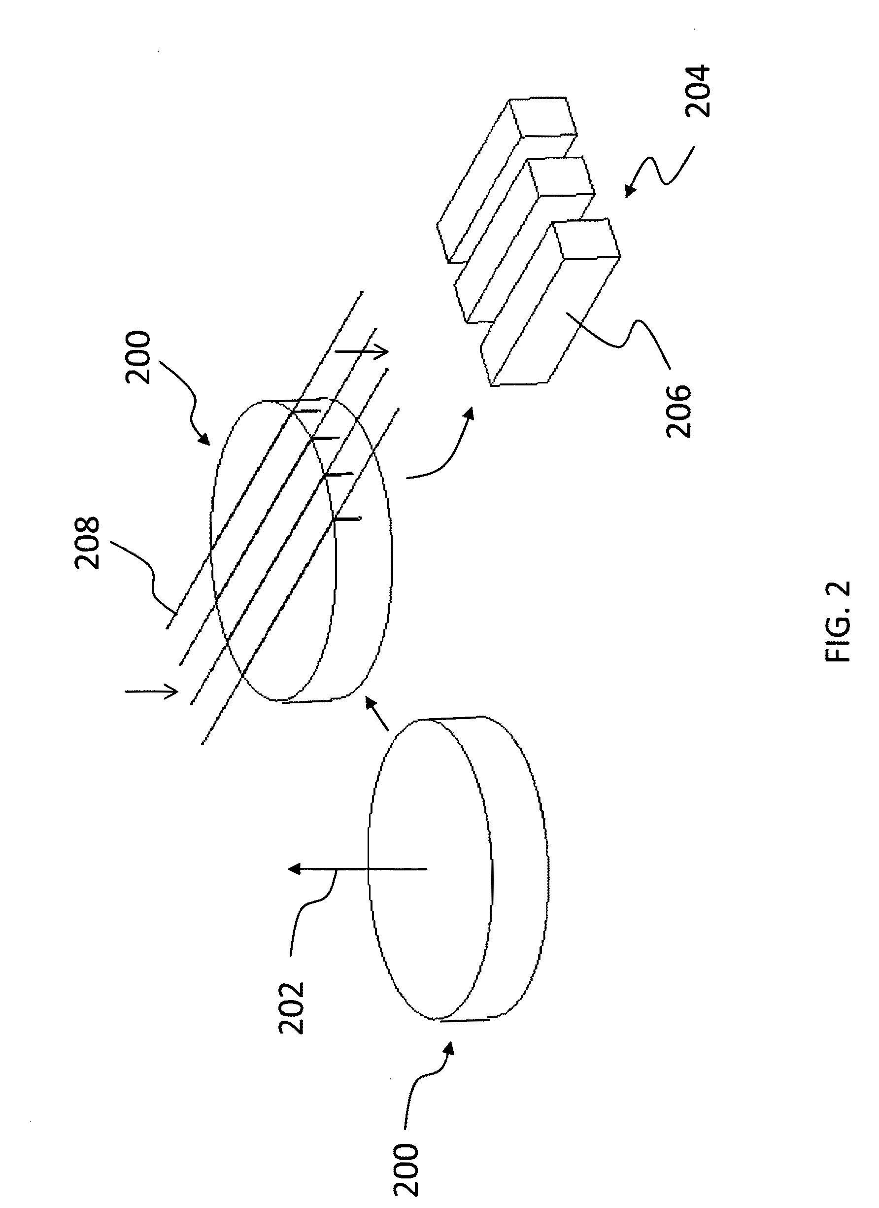
[0042]The following example is provided to illustrate an embodiment of the invention. Using the HVPE growth process, non-polar seed crystals were generated through the growth of thick GaN boules grown on AlN nucleation layers on sapphire substrates. These boules were grown to a thickness of ˜1 cm. The sapphire substrates may be subsequently removed by any suitable technique. FIG. 2 is a schematic representation of an as-grown GaN boule 200 without the underlying sapphire and AlN nucleation layer. The growth of the GaN crystal along the c-axis ([0001] direction) to a thickness of, for example, about 1 cm, is indicated by an arrow 202. Following fabrication of the boules 200, they were prepared for slicing along the c-axis to create a- and m-plane substrates 204. The GaN crystalline directions in each boule 200 were identified via X-ray diffraction prior to slicing on a fixed-abrasive multi-wire saw. The sample boule 200 was mounted on an adjustable fixture in an X-ray diffractometer ...

example 2

[0053]The following example is provided to illustrate another embodiment of the invention. The GaN boules and non-polar seed crystals formed pursuant to this example may be formed as described above in conjunction with FIGS. 2 and 3, and thus can be expected to exhibit the same or similar excellent properties and characteristics mentioned below for this example. Accordingly, the HVPE growth process may again be utilized used to generate non-polar seed crystals through the growth of thick GaN boules grown on AlN nucleation layers on sapphire substrates. GaN boules may be grown to a thickness of, for example, ˜1 cm. Following fabrication of the boules, they are prepared for slicing along the c-axis to create m-plane substrates. The GaN crystalline directions in the boule are identified via X-ray diffraction prior to slicing on a fixed-abrasive multi-wire saw. For the alignment measurement, the boule is mounted on an adjustable fixture in an X-ray diffractometer and the orientation of ...

example 3

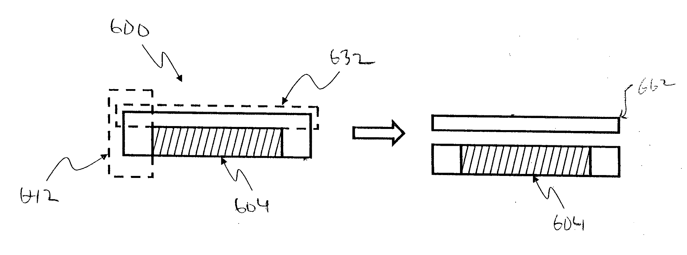
[0061]The following example is provided to illustrate another embodiment of the invention. As in the case of the implementations of Example 2, the GaN boules and non-polar seed crystals formed pursuant to the present example may be formed as described above in conjunction with FIGS. 2 and 3, and thus can be expected to exhibit the same or similar excellent properties and characteristics mentioned above. Accordingly, the HVPE growth process may again be utilized to generate non-polar seed crystals through the growth of thick GaN boules using the process previously described. For example, the size of the m-plane substrates resulting from slicing the GaN boule, and following preparatory steps as described above, may be approximately 5 mm in the [0001] direction and 10 mm in the [1120] direction, and approximately 450 μm thick in the [1100] direction. These substrates may then be utilized as seed crystals for the re-growth process. FIG. 8 schematically depicts a top surface 816 of one s...


PUM


Abstract

Non-polar or semi-polar (Al, Ga, In)N substrates are fabricated by re-growth of (Al, Ga, In)N crystal on (Al, Ga, In)N seed crystals, wherein the size of the seed crystal expands or is increased in the lateral and vertical directions, resulting in larger sizes of non-polar and semi-polar substrates useful for optoelectronic and microelectronic devices. One or more non-polar or semi-polar substrates may be sliced from the re-grown crystal. The lateral growth rate may be greater than the vertical growth rate. The seed crystal may be a non-polar seed crystal. The seed crystal may have crystalline edges of equivalent crystallographic orientation

Description

CROSS-REFERENCE TO RELATED APPLICATIONS[0001]This application claims the benefit of U.S. Provisional Patent Application Ser. No. 60 / 993,867, filed Sep. 14, 2007, titled “Large-area, Non-polar and Semi-polar GaN Substrates, Devices, and Articles, and Methods for Making Them,” the content of which is incorporated by reference herein in its entirety.FEDERALLY SPONSORED RESEARCH[0002]This invention was made with government support under grant number W911NF-06-C-0154 by the U.S. Army. The United States Government may have certain rights in the invention.BACKGROUND OF THE INVENTION[0003]1. Field of the Invention[0004]This invention relates to large-area, non-polar and semi-polar gallium nitride (Al, Ga, In)N substrates useful for producing optoelectronic devices (such as light emitting diodes (LEDs), laser diodes (LDs) and photodetectors) and electronic devices (such as diodes and field effect transistors (FETs)) composed of III-V nitride compounds, and to methods for producing such artic...

Claims


Application Information

Patent Timeline
Patent Type & Authority Applications(United States)
IPC IPC(8): H01L21/205H01L33/00H01L33/16
CPCC30B25/00C30B29/406H01L33/16H01L21/02433H01L33/0075H01L21/02389
Inventor HANSER, ANDREW DAVIDPREBLE, EDWARD ALFREDLIU, LIANGHONGCLITES, TERRY LEEEVANS, KEITH RICHARD
Owner KYMA TECH
Why Eureka
Try Eureka