Method for manufacturing semiconductor device

a manufacturing method and technology for semiconductor devices, applied in semiconductor/solid-state device manufacturing, basic electric elements, electric devices, etc., can solve problems such as defective contact formation, and pattern tilting of amorphous carbon hard masks. achieve high anisotropy

Inactive Publication Date: 2009-03-26
ELPIDA MEMORY INC
View PDF9 Cites 244 Cited by
  • Summary
  • Abstract
  • Description
  • Claims
  • Application Information

AI Technical Summary

Benefits of technology

[0022]According to the present embodiments, when the amorphous carbon film is processed to have a hard mask shape, the side etching of the amorphous carbon film can be prevented and a vertical shape that has a high anisotropy can be obtained, by processing the amorphous carbon film, forming the protective film on the sidewall of the amorphous carbon film, in the middle of the processing, and further processing the amorphous carbon film.

Problems solved by technology

In addition, if amorphous carbon hard mask 3a has such a bowing shape, contact hole 7 tends to have a bowing shape as shown in FIG. 5D, and a problem wherein the defective contact is formed is also caused.
When the amorphous carbon hard mask is processed to have a fine linear pattern, a problem wherein the slimming of the pattern occurs and a desired pattern cannot be obtained is caused.
In the fine linear pattern, there is concern that the pattern tilting of the amorphous carbon hard mask when the substrate to be processed is etched.
Furthermore, in any of fine linear patterns and opening patterns, the problem of pattern deformation may also be caused when the substrate to be processed is etched.

Method used


Image

  • Method for manufacturing semiconductor device
  • Method for manufacturing semiconductor device
  • Method for manufacturing semiconductor device

Examples


first exemplary example

[0030]In the first exemplary example, there is provided a method for manufacturing a semiconductor device that includes:

[0031](A) forming a silicon-free amorphous carbon film on a substrate to be processed, and forming an intermediate mask layer comprising at least a silicon dioxide film on the amorphous carbon film;

[0032](B) processing the intermediate mask layer into an intermediate mask shape;

[0033](C) etching a part of the amorphous carbon film using the processed intermediate mask layer as a mask to expose a sidewall of the amorphous carbon film;

[0034](D) sputtering the intermediate mask layer to form a protective film comprising a silicon oxide on the sidewall of the amorphous carbon film;

[0035](E) further etching the amorphous carbon film until the substrate to be processed is exposed by using the remaining intermediate mask layer and the protective film as a mask; and

[0036](F) processing the substrate to be processed using the amorphous carbon film as a mask.

[0037]The above ...

second exemplary example

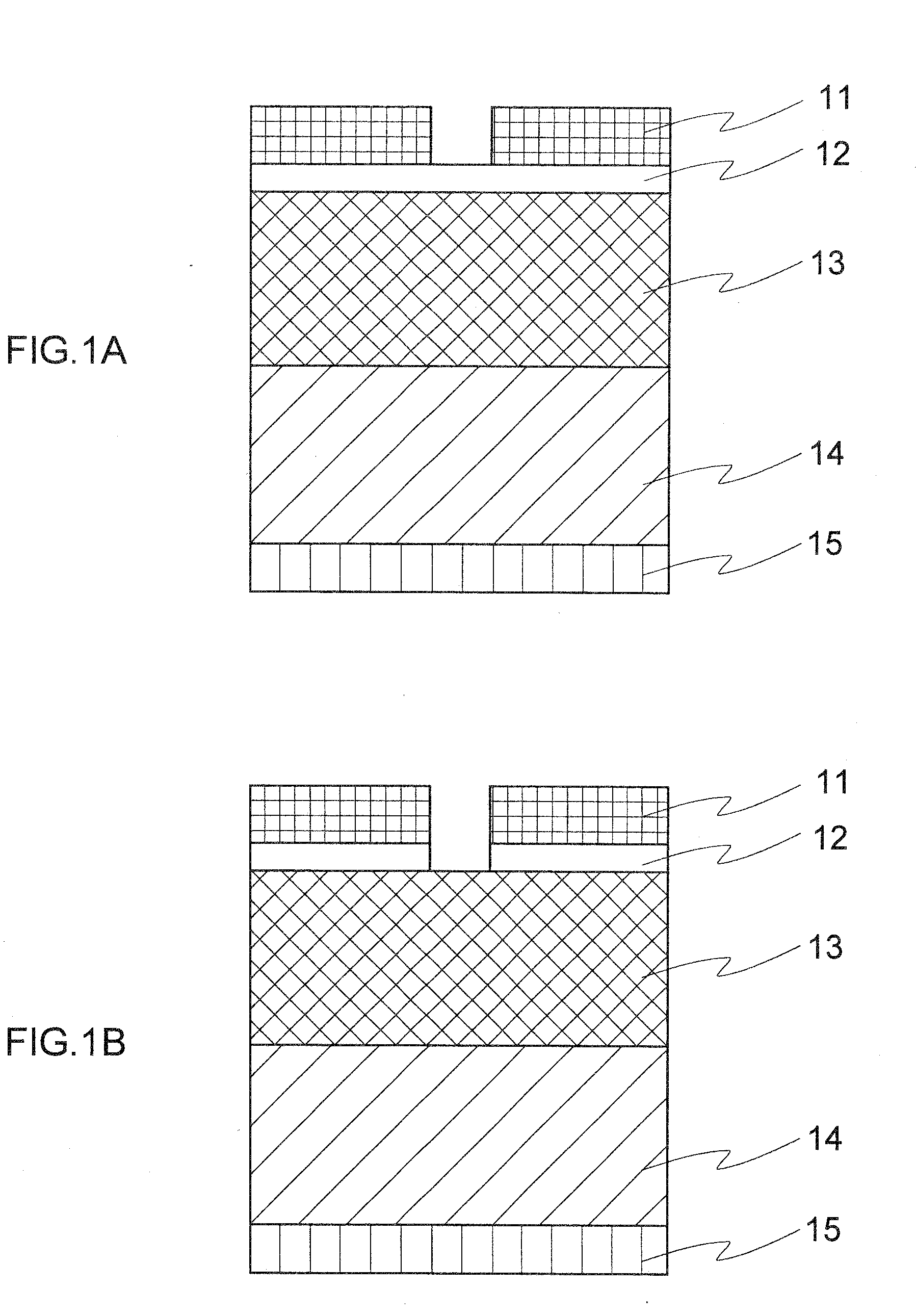
[0051]A manufacturing method for a second exemplary example will be described referring to FIGS. 2A to 2F.

[0052]First as shown in FIG. 2A, silicon nitride film 24, amorphous carbon film 23, and intermediate mask layer 22 are formed on wiring material 25 using CVD, and wiring resist pattern 21 is formed using lithography. Intermediate mask layer 22 is a laminated film of a silicon oxynitride film and a silicon oxide film formed by plasma CVD, and the thicknesses of the silicon oxynitride film and the silicon oxide film are 10 to 30 nm and 30 to 100 nm, respectively.

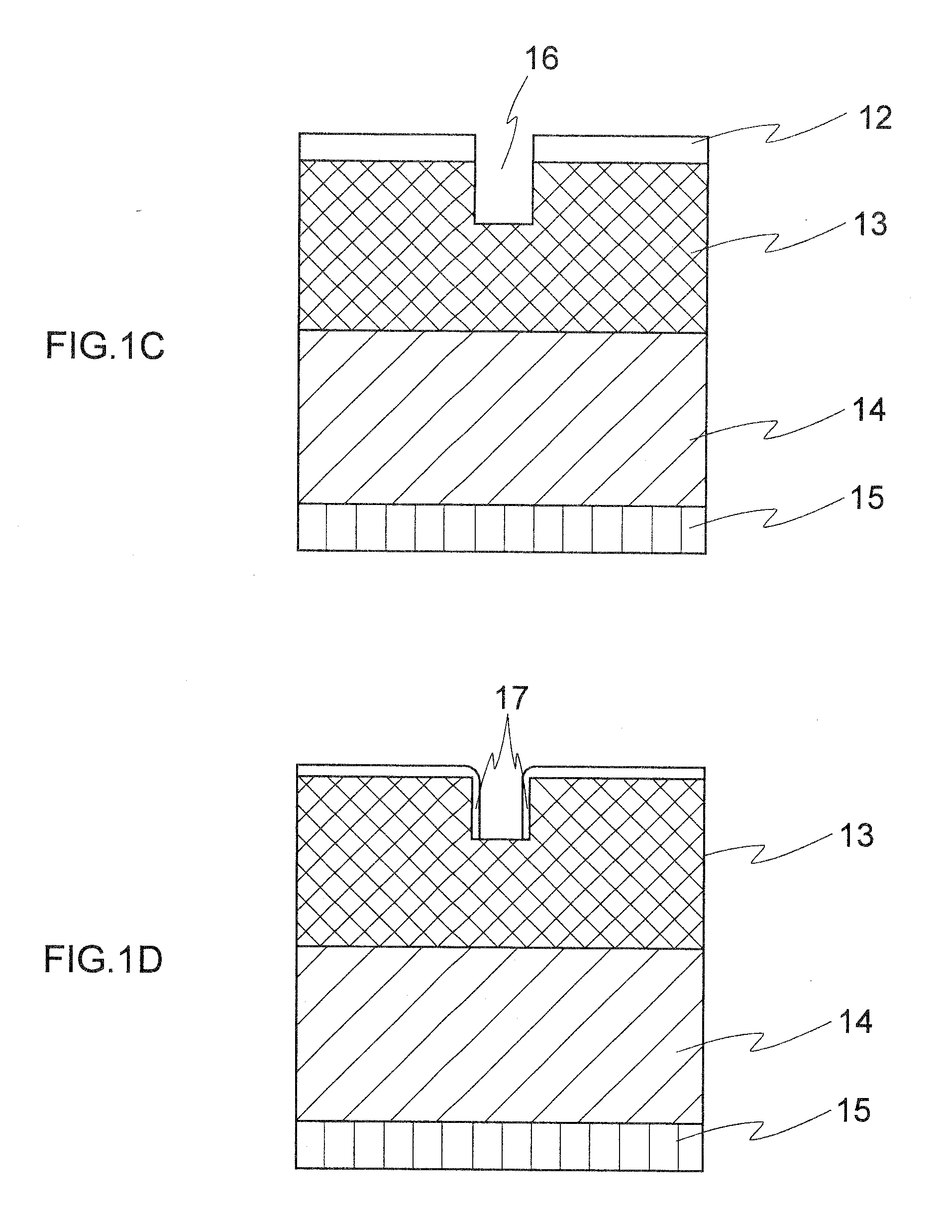
[0053]Next, using a magnetized RIE dry etching apparatus of an RF frequency of 13.56 MHz shown in FIG. 4, intermediate mask layer 22 and amorphous carbon film 23 are processed. CF4 is used as the etching gas for intermediate mask layer 22, the chamber pressure is controlled at 4.0 to 20.0 Pa (30 to 150 mTorr), the RF power is set between 300 and 2,000 W, and the stage temperature is 0 to 60° C. After etching, intermediate ...

third exemplary embodiment

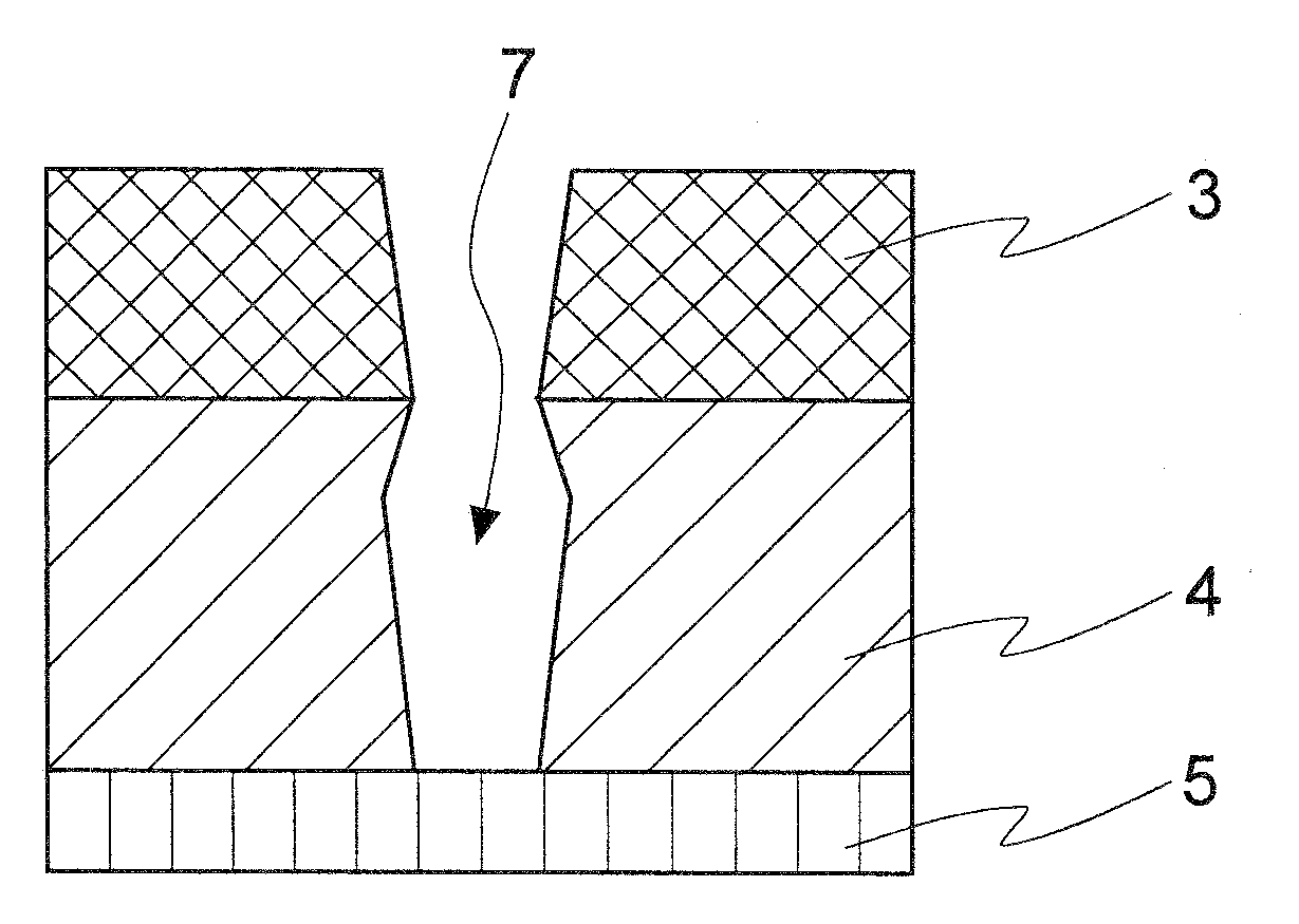
[0059]Even when the thickness of the amorphous carbon film is not excessively thick, and slimming does not cause major problems, the formation of a protective film by the sputtering of the intermediate mask layer can be used in order to improve the pattern accuracy.

[0060]After processing to the state shown in FIG. 2B in the same manner as described above, amorphous carbon film 23 is etched as shown in FIG. 3A.

[0061]Next, as shown in FIG. 3B, intermediate mask 22a is sputtered by etching using a gas system that contains no oxygen to form protective film 22c of the oxide on the sidewall of amorphous carbon film 23. Thereafter, in the same manner as described above, silicon nitride film 24 is processed by dry etching using a fluorine-containing gas such as CF4 gas, and a bottom layer produced during the etching of silicon nitride film 24 by is removed using oxygen gas so that the transferring the pattern to silicon nitride film 24 is completion.

[0062]By thus protecting the amorphous ca...


PUM

PropertyMeasurementUnit
pressureaaaaaaaaaa
pressureaaaaaaaaaa
temperatureaaaaaaaaaa

Abstract

There is provided a method for manufacturing a semiconductor device including processing a substrate to be processed by using an amorphous carbon hard mask that includes processing an amorphous carbon film formed on the substrate to be processed to provide a hard mask, and forming a protective film comprising a silicon oxide film on a sidewall of the amorphous carbon film exposed during or after processing the amorphous carbon film; and the protective film preferably formed by sputtering an intermediate mask comprising at least a silicon oxide on the amorphous carbon film.

Description

BACKGROUND OF THE INVENTION[0001]1. Field of the Invention[0002]The present invention relates to a method for manufacturing a semiconductor device, and more specifically, to a method for manufacturing a semiconductor device that uses an amorphous carbon film as a hard mask.[0003]2. Description of Related Art[0004]With the progress of the semiconductor micro-fabrication techniques in recent years, an ArF resist that is patterned by short-wavelength light has been increasingly used. The ArF resist has low dry-etching resistance and is formed into a thin film due to shallow depth of focus. Therefore, a hard mask that has high dry-etching resistance and thick film thickness is required, and techniques that use amorphous carbon or the like as the material for the hard mask have been disclosed (for example, Japanese Patent Application Laid-Open No. 2002-194547).[0005]FIGS. 5A to 5D are process sectional views that show a method for manufacturing a conventional semiconductor device using a...

Claims


Application Information

Patent Timeline
Patent Type & Authority Applications(United States)
IPC IPC(8): H01L21/302
CPCH01L21/31116H01L21/31144H01L21/31122
Inventor SUKEKAWA, MITSUNARI
Owner ELPIDA MEMORY INC
Why Eureka
Try Eureka