Copper Indium Diselenide-Based Photovoltaic Device And Method Of Preparing the Same

a technology of copper indium diselenide and photovoltaic device, which is applied in the field of photovoltaic device, can solve the problems of limited application limited use of cis-based photovoltaic device substrate, and typical rigidity of glass devices, and achieve the effect of maximum device efficiency

Inactive Publication Date: 2009-04-02
ITN ENERGY SYST INC +1
View PDF31 Cites 33 Cited by
  • Summary
  • Abstract
  • Description
  • Claims
  • Application Information

AI Technical Summary

Benefits of technology

[0008]The present invention provides a copper indium diselenide (CIS)-based photovoltaic device and a method of preparing the same. The CIS-based device includes a CIS-based solar absorber layer which is based on copper, indium, and selenium, and optionally includes alloys with aluminum, gallium and sulfur. The CIS-based photovoltaic device further includes a substrate formed from a silicone composition. The substrate, because it is formed from the silicone composition, is both flexible and sufficiently able to withstand annealing temperatures in excess of 500° C. to obtain maximum efficiency of the device.

Problems solved by technology

To date, the CIS-based photovoltaic devices have been limited in the applications for which they may be used due to an inverse correlation between versatility and efficiency.
To date, few materials have proven useful for the substrate in the CIS-based photovoltaic devices due to an inability to sufficiently resist cracking and mechanical failure at the annealing temperatures in excess of 500° C. Various types of glass are predominantly used as the substrate; however, glass adds weight to the devices and is typically rigid.
The rigidity of the glass substrates renders the devices unsuitable for applications that require flexibility or applications in which the devices may be subjected to blunt force that could crack or otherwise damage the glass substrates.
In addition to limiting potential applications for the devices, the glass substrates also require that the devices be individually prepared.
The polyimide substrates eliminate the deficiencies of the glass substrates as to excessive weight and inflexibility; however, the polyimide substrates are prone to severe degradation at temperatures in excess of 425° C. resulting in cracking and mechanical failure of devices.
As such, the devices including the polyimide substrate cannot be properly formed to maximize efficiency of the devices.

Method used


Image

  • Copper Indium Diselenide-Based Photovoltaic Device And Method Of Preparing the Same
  • Copper Indium Diselenide-Based Photovoltaic Device And Method Of Preparing the Same
  • Copper Indium Diselenide-Based Photovoltaic Device And Method Of Preparing the Same

Examples


example 1

Preparation of Fiber Reinforced Substrates from MP101 Crystal Coat Resin

[0210]A four-inch wide saturation trough was used. Style 106 glass fabric, obtained from BGF Industries and heat cleaned in air, was cut into strips 15″×3.5″ in size. Approximately 7 ml of the MP101 resin, available from SDC Technologies, Inc., was placed in the saturation tough and the glass fabric was drawn through the resin solution to form an impregnated fiber reinforcement. The impregnated fiber reinforcement was hung vertically in a fumed hood to dry and then transferred to an air-circulating oven to cure. The impregnated fiber reinforcement was partially cured at 50° C. for 10 min. and then impregnated again with the same resin. After drying, the impregnated fiber reinforcement was cured by the following procedure: 1° C. / min. to 75° C., 75° C. / 1 h., 1° C. / min. to 100° C., 100° C. / 1 h., 1° C. / min. to 125° C., and 125° C. / 1 h to form the fiber reinforced substrate. The fiber reinforced substrate was kept in...

example 2

Preparation and Properties of Fiber Reinforced Substrates from the MP101 Crystal Coat Resin and 0.2 wt % Treated Pyrograf III

[0211]0.031 grams of oxidized Pyrograf III was mixed into 50 grams of MP101 Crystal Coat resin in a glass vial and placed in a Bransonic ultrasonic cleaning bath and dispersed for 30 minutes. The mixture was then centrifuged if there was un-dispersed powder and the top dispersion was taken for film preparation.

[0212]The Style 106 glass fabric was heat, cleaned, and cut into a shape that would fit into the saturation pan. The mixture of the Pyrograf III and MP101 Crystal Coat resin was placed in the saturation pan, and the fabric was passed through the mixture in the saturation pan to form an impregnated fiber reinforcement. The impregnated fiber reinforcement was hung vertically in a fumed hood to dry and then transferred to an air-circulating oven to cure by the following procedure: 1° C. / min. to 75° C., 75° C. / 1 h., 1° C. / min. to 100° C., 100° C. / 1 h., 1° C....

example 3

Fabrication and Testing of CIGS (Copper Indium Gallium Diselenide)-Based Photovoltaic Devices on Substrates Prepared from Example 1

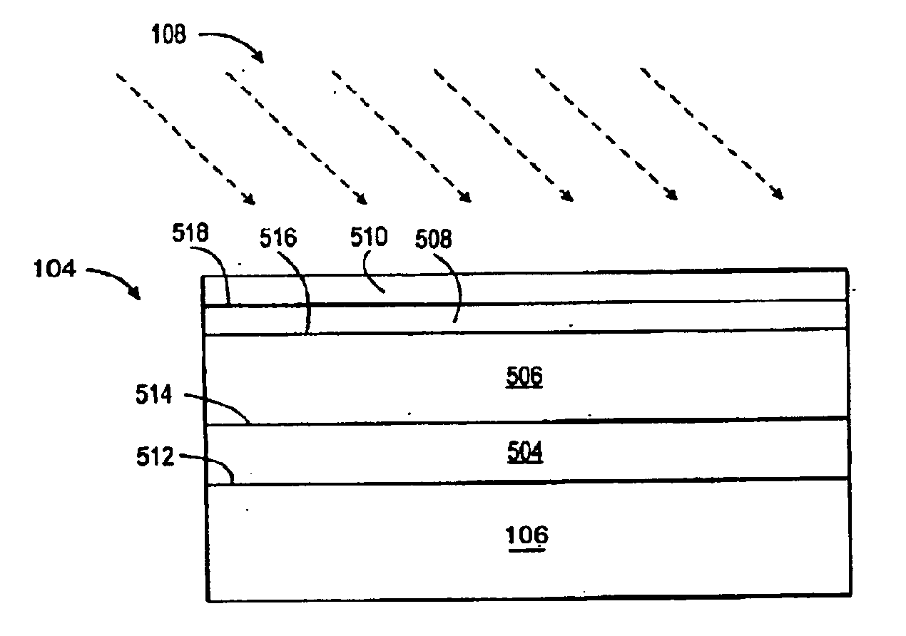
[0213]An approximately 0.5 micrometer thick layer of molybdenum was sputtered onto the fiber reinforced substrate prepared in Example 1. Copper, indium, and gallium were co-evaporated onto the layer of molybdenum in a selenium atmosphere at a deposition substrate temperature of about 575° C. for 20 minutes to form a CIS-based solar absorber layer having a thickness of about two micrometer thick. A 50 nm layer of CdS was then deposited onto the CIGS layer through a wet CBD bath process to form a window layer. A ZnO electrically insulating layer and an ITO top contact layer were sputtered onto the window layer and then nickel-silver grids were evaporated onto the top contact layer. The cell performance was tested under AM1.5 illumination condition and an efficiency of 1 to 2% was measured.


PUM

PropertyMeasurementUnit
temperatureaaaaaaaaaa
temperaturesaaaaaaaaaa

Abstract

A copper indium diselenide (CIS)-based photovoltaic device includes a CIS-based solar absorber layer including copper, indium, and selenium. The CIS-based photovoltaic device further includes a substrate formed from a silicone composition. The substrate, because it is formed from the silicone composition, is both flexible and sufficiently able to withstand annealing temperatures in excess of 500° C. to obtain maximum efficiency of the device.

Description

RELATED APPLICATIONS[0001]This patent application claims priority to and all advantages of U.S. Provisional Patent Application Nos. 60 / 792,871 and 60 / 792,852, both filed on Apr. 18, 2006.FIELD OF THE INVENTION[0002]The present invention generally relates to a copper indium diselenide-based photovoltaic device and a method of preparing the photovoltaic device. More specifically, the invention relates to a photovoltaic device that includes a polymeric substrate.BACKGROUND OF THE INVENTION[0003]Copper indium diselenide (CIS)-based photovoltaic devices are well known for generating electricity from sunlight and other sources of light. The CIS-based photovoltaic devices are useful for providing electricity for any application in which the devices are exposed to the source of light. As a result, the potential applications for CIS-based photovoltaic devices are far-reaching.[0004]To date, the CIS-based photovoltaic devices have been limited in the applications for which they may be used du...

Claims


Application Information

Patent Timeline
Patent Type & Authority Applications(United States)
IPC IPC(8): H01L31/042H01L31/00H01L31/072
CPCC08G77/12H01L31/046C08G77/20C08L83/04C09D183/04H01L31/0322H01L31/0392H01L31/03928H01L31/072H01L31/0749Y02E10/541C08G77/14C08L83/00H01L31/0463H01L31/0465H01L31/03925Y02P70/50H01L31/032H01L31/0336
Inventor ANDERSON, NICOLE R.KATSOULIS, DIMITRIS ELIASREESE, HERSCHEL HENRYZHU, BIZHONGWOODS, LAWRENCE M.ARMSTRONG, JOSEPH H.RIBELIN, ROSINE M.
Owner ITN ENERGY SYST INC
Why Eureka
Try Eureka