Scalable mass data storage device

a data storage device and mass data technology, applied in the field of scalable mass data storage devices, can solve the problems of low cost of hdds, severe limitations, and severe failures of current data storage devices, and achieve the effects of facilitating concurrency of operations, increasing volumetric density, and increasing data transfer rates

Active Publication Date: 2009-04-09
STACKSPEED INC +1
View PDF46 Cites 45 Cited by
  • Summary
  • Abstract
  • Description
  • Claims
  • Application Information

AI Technical Summary

Benefits of technology

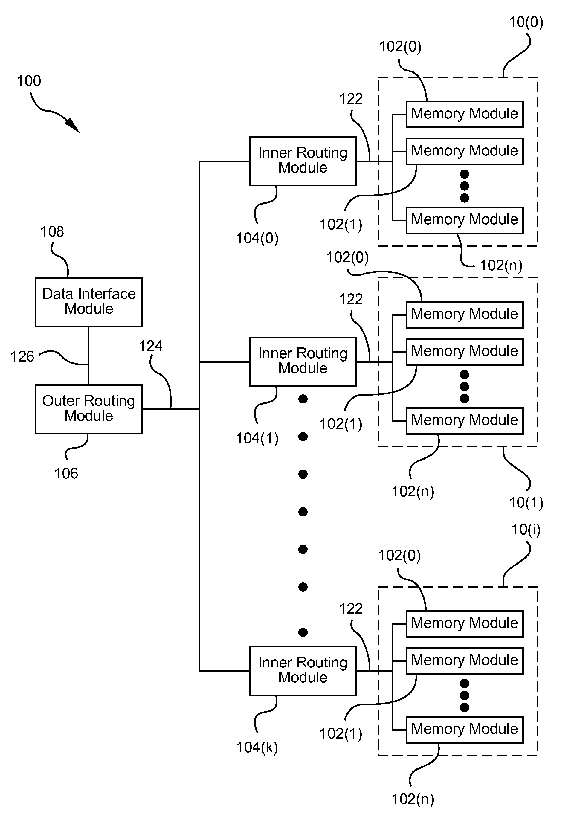
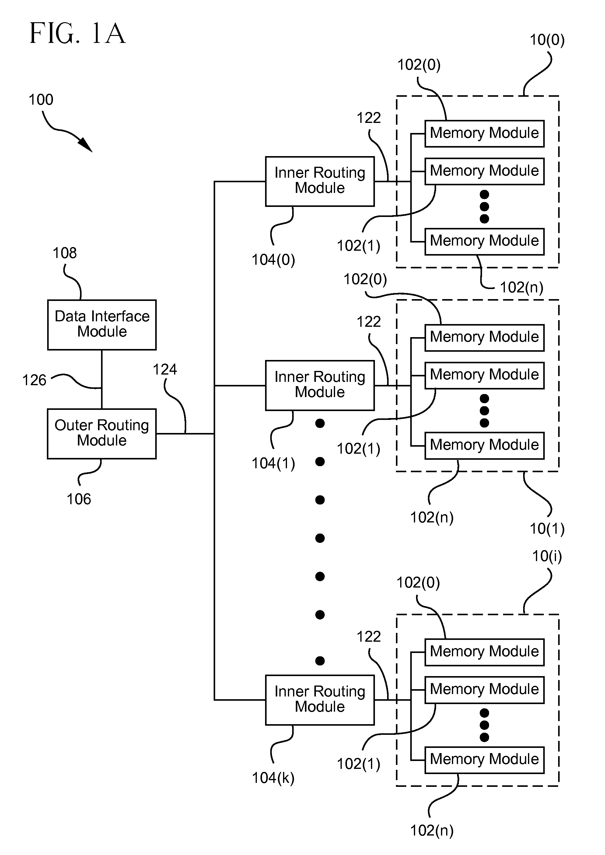
[0017]The present invention involves a scalable data storage device, which includes non-volatile memory, uses a networked bus system and can be solid-state or MEMS-based. The scalable data storage device of the present invention uses data routing modules which are adapted to store incoming data and send outgoing data thereby providing decoupling of the networked buses. This arrangement enables significantly higher data transfer rates, surpassing DRAM SSDs at a fraction of the size and cost, provides increased volumetric density (1 TB in less than 1 cubic inch), and permits concurrency of operations. The scalable data storage device of the present invention can be engineered to have a rewrite capability of over 500 times that of Flash RAM: and can scale down to 8 bits and up to exabytes, yottabytes and beyond. The scalable data storage device of the present invention may be used in a wide range of applications from large data centers to small consumer electronic products. The data storage device of the present invention is designed to use currently well developed, proven components with scientific principles that are also well understood to implement the data storage device as a chip, a multi-chip package (MCP), or as part of a System-on-a-Chip (SoC) integrating the data storage device with other devices in a single logical package.

Problems solved by technology

Current data storage devices have severe limitations.
However, HDDs apparent low cost comes with severe failings and limitations.
HDDs are not solid state and the relative low cost of HDDs comes with many failings.
Due to the mechanical nature of HDDs and the configuration of the disks and the heads, HDDs are inherently fragile.
HDDs are particularly vulnerable to damage from sudden mechanical shocks, which may cause the disks to collide with the heads.
The necessity of thin platters in an effort to reduce power consumption and inertia, combined with bringing the read / write head ever closer to the platter for increased data density makes the head crashes increasingly inevitable.
As a result, a drop of even a few feet can have devastating effects on the lifetime of an HDD.
The volume space of the same heads and platters that cause the fragility and unreliability also prevent HDDs from achieving significant volumetric density, with the most capacious HDDs (1 TB drive in a standard 3.5 inch drive form factor) only delivering 39.5 GB per cubic inch.
Additionally, the power consumption from moving the heads and spinning the platters is also of major concern.
Modern HDDs can consume 20 watts of power when running simply because it takes that much power to keep the platters spinning at the appropriate speed and to move the stack of heads at the extreme speeds needed.
This power consumption drives the real cost of an HDD up substantially, making them, in fact, sometimes more expensive than other technologies.
In fact, most HDDs are rated at about 28 to 30 decibels, making them difficult for many people to accept in various environments, including, among others, quiet environments such as media center computers.
While HDDs have made progress in apparent concurrency with the near universal introduction of command queuing, the fact remains that this simply allows the drive to reorder instructions for improved performance, and no currently available drive offers real concurrency of operations.
This would require multiple heads per platter, which is something that would raise the costs of HDDs to unacceptable levels.
This means that no matter how inexpensive HDDs appear, they are at best antiquated technology.
Further, there is no foreseeable method for HDDs to do anything but fall further behind.
It would seem apparent that many of these flaws would go away by moving to a solid-state drive (SSD), but that is not necessarily the case.
In Flash-based SSDs, many of the problems associated with HDDs remain.
Generally available Flash SSDs suffer the major flaw of being almost entirely consecutive in operation and therefore incapable of concurrent operations.
This creates major problems for Flash SSDs moving forward as the performance is limited by these designs, keeping Flash SSDs limited to only those areas that do not require great amounts of speed or capacity.
Flash SSDs are solid-state, so they do not suffer from fragility as do HDDs, but the internal design and independent cell speed prevents them from currently operating faster than approximately 32 MB / sec, making Flash SSDs the slowest data storage technology in widespread use today.
Although Flash SSDs are used primarily because they allow for the smallest form factor, the total volumetric density of Flash SSDs is poor.
Further, the volumetric density will remain low due to the fact that flash chips contain more resin than flash cells, leaving the highest capacity Flash SSD available today with a total volumetric density of only 14.9 GB per cubic inch.
Also, Flash SSDs wear out faster than HDDs, ie., they have a shorter life.
Flash cells have a well established problem that each time a cell is written, the cell degrades a small amount.
Flash chips have write balancing in order to help combat this, but file usage in a computer system actually works against the write balancing.
Since the vast majority of files are written once in the lifetime of the computer, the write balancing only balances between a very limited number of pages, resulting in those pages becoming exhausted.
Furthermore, Flash SSDs do not scale.
In view of the way the internal structures are designed, the only method to increase capacity without massive reengineering is to attach multiple dies to a single bus, thereby increasing the parasitic drains and capacitances that eventually slow the entire chip to the point where it becomes unusable.
As a result, either small capacity Flash SSD have to be accepted or larger Flash dies have to be built, which in turn raises the cost per functioning cell.
Even with multiple separately manufactured dies, the internal design of Flash SSDs prevent concurrency, providing no ability to perform multiple tasks at once, and limiting performance in yet another dimension.
These limitations and the associated costs have led many organizations to use Flash ICs directly, instead of a complete Flash SSD.
This usage has exactly the same problems, but in some instances can reduce the per unit monetary costs by a small amount.
By far the largest flaw is price.
To expand capacity, manufacturers add additional DRAM chips to one of a small number of buses and each new chip lowers the performance of that bus a small amount, until the entire system noticeably slows down.
Additionally, a DRAM SSD can consume 2400 watts of power per TB making it the most costly data storage technology in terms of power consumption as well.
Consuming so much power, it is necessary to have substantial cooling fans to dissipate the heat produced, adding not just noise, often louder than HDDs, but also adding moving components that can fail leading to destruction of the data on the DRAM SSD.
Thus, DRAM SSDs are simply unsuitable for the vast majority of situations, and are only considered as an option when the raw performance is so critical as to be worth the enormous costs in equipment, power consumption, air conditioning, volatility, space and noise.
In sum, no current data storage technology provides high volumetric density (data capacity per volume of space).
No current data storage technology provides scalability.
No current data storage technology provides substantial concurrency.
No current data storage technology provides a viable technology to meet the demands of the future.

Method used


Image

  • Scalable mass data storage device
  • Scalable mass data storage device
  • Scalable mass data storage device

Examples


Embodiment Construction

[0063]The data storage devices formed in accordance with the present invention can have scalable architectures with high density data storage capacity and high data transfer rates. In this manner, the data storage devices of the present invention are scalable in storage capacity and data transfer speed without requiring any fundamental re-engineering. The data storage devices can be implemented using relatively small form factors, while achieving a large data storage capacity. The data storage devices can be composed of solid state components that can be integrated in a single package or may be implemented using multiple packages. One or more of the components of the data storage devices can be implemented on a single semiconductor die.

[0064]The scalable architectures of the data storage devices allow the storage capacity of the data storage device to be increased or decreased without having to completely redesign the data storage devices. In addition, preferred architectures of the...


PUM


Abstract

A scalable data storage device which includes non-volatile memory uses a networked bus system which can be employed on a single memory storage chip level or in a multi-chip package (MCP). The scalable data storage device uses data routing modules which are adapted to store incoming data and send outgoing data thereby providing decoupling of the networked buses. This arrangement enables significantly higher data transfer rates, surpassing DRAM SSDs at a fraction of the size and cost, provides increased volumetric density (1 TB in less than 1 cubic inch), and permits concurrency of operations. The scalable data storage device can be engineered to have a rewrite capability of over 500 times that of Flash RAM and can scale down to 8 bits and up to exabytes, yottabytes and beyond. The scalable data storage device may be used in a wide range of applications from large data centers to small consumer electronic products.

Description

BACKGROUND[0001]Current data storage devices have severe limitations. Hard Disk Drives (HDDs) are the default mass data storage technology of choice for the majority of applications: datacenters, desktops, laptops, media center computers, and some consumer electronic products. This widespread use stems from being a low cost solution. However, HDDs apparent low cost comes with severe failings and limitations.[0002]HDDs are not solid state and the relative low cost of HDDs comes with many failings. HDDs are implemented using a stack of disks, also referred to as platters, on which regions are magnetized with different polarities to represent data being stored. The disks spin on a spindle and can be read from or written to using a head. Each side (top and bottom) of a given disk has a corresponding head for reading and writing data, with all heads tied to a single armature. Due to the mechanical nature of HDDs and the configuration of the disks and the heads, HDDs are inherently fragil...

Claims


Application Information

Patent Timeline
Patent Type & Authority Applications(United States)
IPC IPC(8): G06F12/00
CPCG06F13/404Y02B60/1235Y02B60/1228Y02D10/00
Inventor ASHWOOD, JOSEPH
Owner STACKSPEED INC
Why Eureka
Try Eureka