Inter-connecting structure for semiconductor package and method of the same

a technology of interconnection structure and semiconductor, which is applied in the direction of semiconductor devices, semiconductor/solid-state device details, electrical apparatus, etc., can solve the problems of poor thermal dissipation performance, inability to meet the demand of producing smaller chips with high density elements on the chip, and inability to meet the demand of producing high-density chips. high density, high reliability package

Inactive Publication Date: 2009-04-16
ADVANCED CHIP ENG TECH
View PDF2 Cites 34 Cited by
  • Summary
  • Abstract
  • Description
  • Claims
  • Application Information

AI Technical Summary

Benefits of technology

[0008]An object of the present invention is to provide a semiconductor device package (chip assembly) with a chip and a conductive trace that provides a low cost, high performance and high reliability package.

Problems solved by technology

As a semiconductor become more complicated, the traditional package technique, for example lead frame package, flex package, rigid package technique, can't meet the demand of producing smaller chip with high density elements on the chip.
Typical BGA packages include a convoluted signal path, giving rise to high impedance and an inefficient thermal path which results in poor thermal dissipation performance.
Further, the solder is typically a tin-lead alloy and lead-based materials are becoming far less popular due to environmental concerns over disposing of toxic materials and leaching of toxic materials into ground water supplies.
Furthermore, because conventional package technologies have to divide a dice on a wafer into respective dies and then package the die respectively, therefore, these techniques are time consuming for manufacturing process.
Since the chip package technique is highly influenced by the development of integrated circuits, therefore, as the size of electronics has become demanding, so does the package technique.
Since these conventional designs include too many stacked dielectric layers, the mechanical property of the dielectric layers involves the “plastic / hardness” property instead of “elastic / softness” due to the CTE of die and molding compound in process concern; and the solder balls are just attached over the RDL, apparently, the design fails to consider the TCT (thermal cycle test), ball-shear test and drop test issues.
Once the device is attached (by SMT process) on the mother board (PCB), the solder balls will be suffered the highest stress in temperature cycling due to the CTE mismatching between PCB and device itself, and either the solder mask (top dielectric layer) or bump reinforced collars can not locked the solder balls firmly (too thin and brittle—easy crack during TCT).
Furthermore, the CTE of the upper dielectric layer is not matching to the CTE of PCB, it means that there is no stress releasing buffer layers to be built inside.
Therefore, the scheme is not reliable during thermal cycle and the operation of the package.

Method used


Image

  • Inter-connecting structure for semiconductor package and method of the same
  • Inter-connecting structure for semiconductor package and method of the same
  • Inter-connecting structure for semiconductor package and method of the same

Examples


Embodiment Construction

[0022]The invention will now be described in greater detail with preferred embodiments of the invention and illustrations attached. Nevertheless, it should be recognized that the preferred embodiments of the invention is only for illustrating. Besides the preferred embodiment mentioned here, present invention can be practiced in a wide range of other embodiments besides those explicitly described, and the scope of the present invention is expressly not limited expect as specified in the accompanying claims.

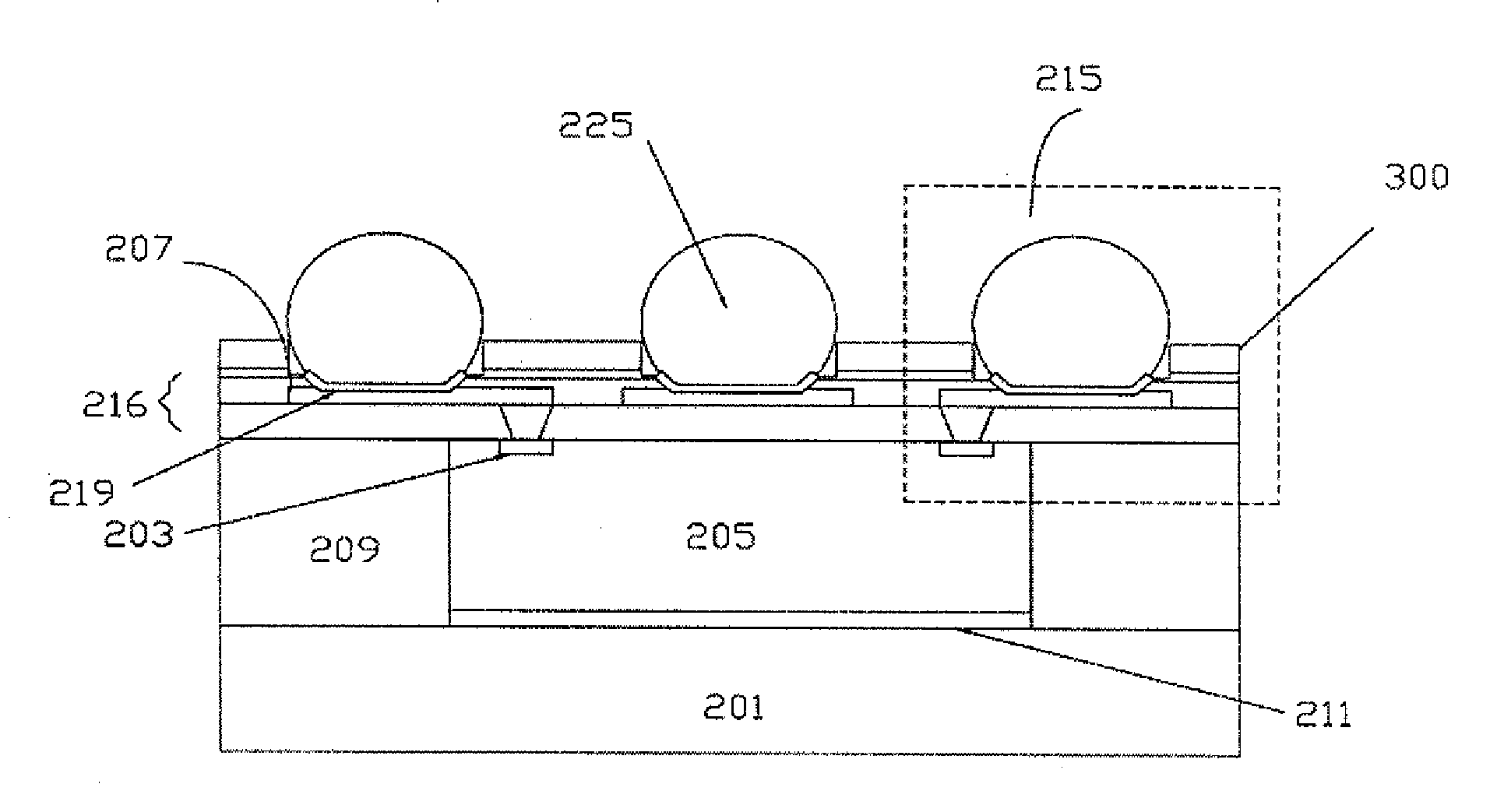
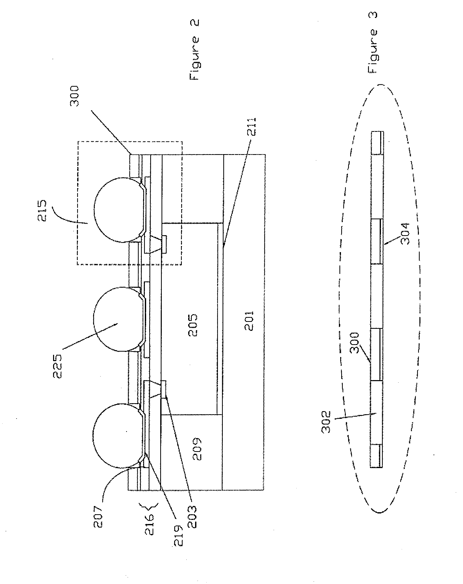
[0023]The present invention discloses a semiconductor device package structure. The present invention provide a semiconductor chip assembly which includes chip, conductive trace and metal inter-connecting as shown in FIG. 2.

[0024]FIG. 2 is cross-sectional view of a substrate 201. The substrate 201 could be a metal, alloy, silicon, glass, ceramic, plastic, PCB or PI. The thickness of the substrate is around 40-200 micron-meters. It could be a single or multi-layer substrate. A chip...


PUM


Abstract

The interconnecting structure for a semiconductor die assembly comprises a build-up layers having RDL formed therein formed over a die having die pads formed thereon, wherein the RDL is coupled to the die pads; an isolation base having ball openings attached over the build-up layer to expose ball pads within the build-up layers; and conductive balls placed into the ball openings of the isolation base and attached on the ball pads within the build-up layers.

Description

FIELD OF THE INVENTION[0001]This invention relates to a semiconductor package, and more particularly to an inter-connecting structure for of package.DESCRIPTION OF THE PRIOR ART[0002]The function of chip package includes power distribution, signal distribution, heat dissipation, protection and support, etc. As a semiconductor become more complicated, the traditional package technique, for example lead frame package, flex package, rigid package technique, can't meet the demand of producing smaller chip with high density elements on the chip. In general, array packaging such as Ball Grid Array (BGA) packages provide a high density of interconnects relative to the surface area of the package. Typical BGA packages include a convoluted signal path, giving rise to high impedance and an inefficient thermal path which results in poor thermal dissipation performance. With increasing package density, the spreading of heat generated by the device is increasingly important. In order to meet pac...

Claims


Application Information

Patent Timeline
Patent Type & Authority Applications(United States)
IPC IPC(8): H01L23/488H01L21/44
CPCH01L23/5389H01L2224/0401H01L2224/04105H01L2224/20H01L2224/73267H01L2924/01013H01L2924/01015H01L2924/01029H01L2924/01033H01L2924/01075H01L2924/01077H01L2924/01078H01L2924/01079H01L2924/01082H01L2924/01327H01L2924/09701H01L2924/14H01L2924/15311H01L2924/3011H01L2924/3025H01L2224/12105H01L2224/32225H01L2224/32245H01L2924/01006H01L24/19H01L2224/16225H01L2924/351H01L2924/181H01L2224/05571H01L2924/00H01L2924/00012
Inventor YANG, WEN-KUNHSU, HSIEN-WEN
Owner ADVANCED CHIP ENG TECH
Why Eureka
Try Eureka