Surface acoustic wave device, and manufacturing method therefor

a surface acoustic wave and a manufacturing method technology, applied in the direction of piezoelectric/electrostrictive transducers, generators/motors, transducer types, etc., can solve the problems of erosion and risk of bad influence, and achieve the effect of high reliability and prevention of idt electrode erosion caused by halogen gas

Inactive Publication Date: 2009-04-16
TAIYO YUDEN KK
View PDF3 Cites 28 Cited by
  • Summary
  • Abstract
  • Description
  • Claims
  • Application Information

AI Technical Summary

Benefits of technology

[0023]Thus, according to the manufacturing method of the present invention, because no halogen gas remains in the hollow sealed by the halogen-free th

Problems solved by technology

Therefore, similarly to the case described in the aforementioned Patent document 2, there is a risk of bad influence such as erosion pro

Method used


Image

  • Surface acoustic wave device, and manufacturing method therefor
  • Surface acoustic wave device, and manufacturing method therefor
  • Surface acoustic wave device, and manufacturing method therefor

Examples


first embodiment

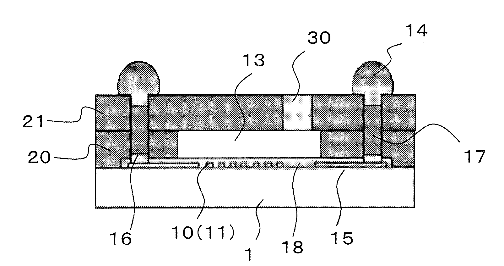
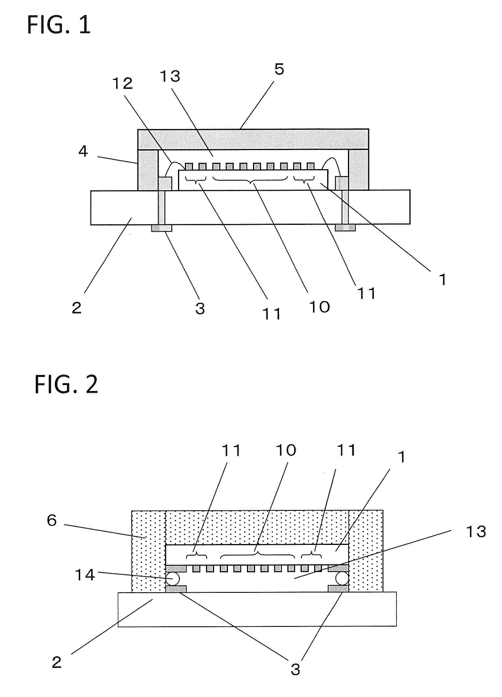
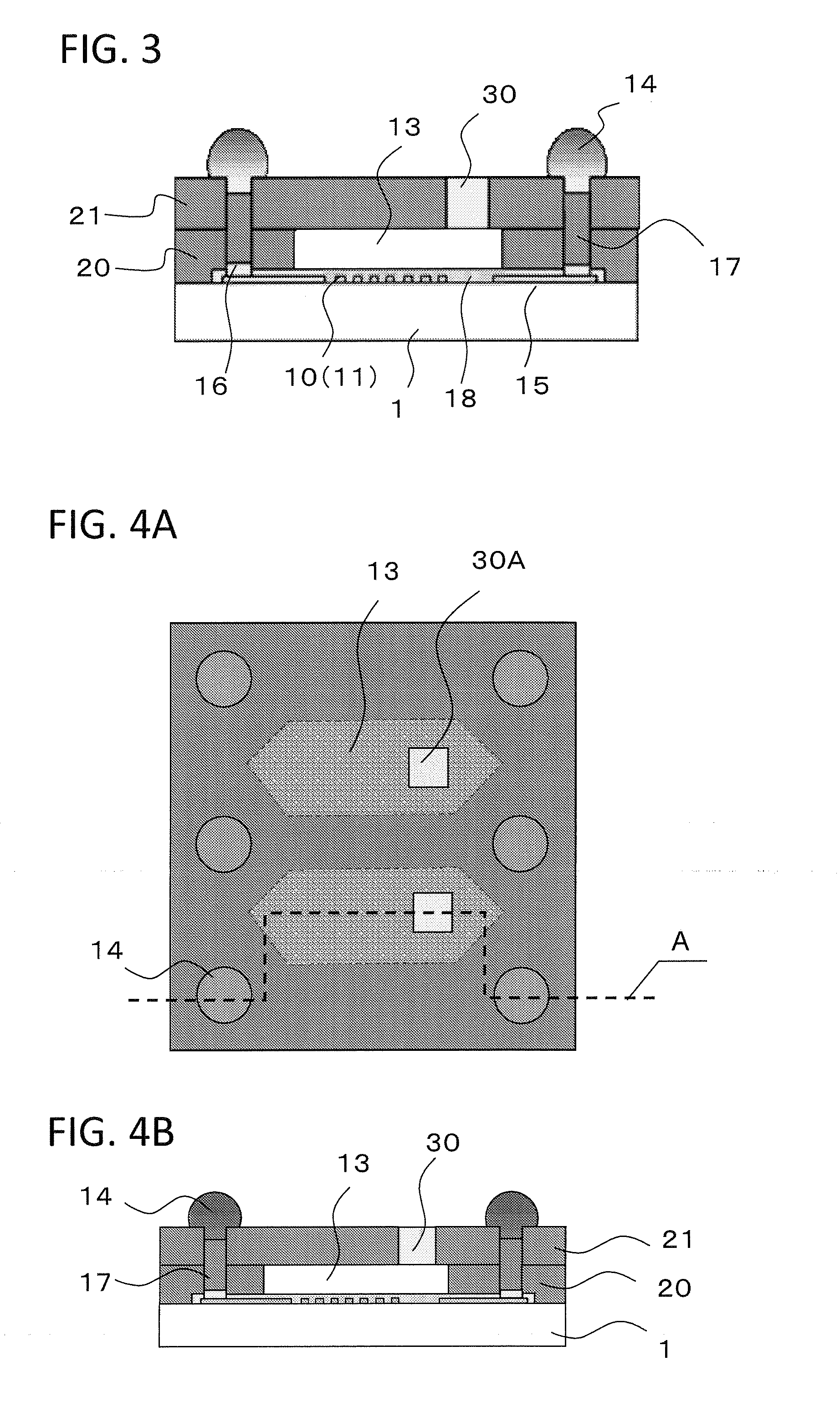
[0035]FIG. 3 shows a diagram illustrating a schematic cross section of a first embodiment of the surface acoustic wave (SAW) device according to the present invention. FIG. 5 is a process diagram explaining the manufacturing process thereof.

[0036]Here, the SAW device shown in the figures represents only one SAW device, on the assumption of a state such that each SAW device is formed by separating a plurality of SAW devices, simultaneously formed on a wafer, into individual pieces by dicing at the completion of manufacturing.

[0037]In FIG. 3, a piezoelectric substrate 1 formed of LiTaO3 etc. is prepared (processing process P1). As the electrode to form surface acoustic wave, on the piezoelectric substrate 1, there are formed an IDT 10 constituted of aluminum alloy of Al—Cu, which is a drive electrode portion to excite surface acoustic wave, and a reflective electrode 11. Also, a wiring electrode 15 for external connection is formed. Further, a protection film 18 constituted of a silic...

second embodiment

[0049]FIG. 6 is a diagram illustrating a schematic cross section of a second embodiment of the SAW device according to the present invention.

[0050]FIG. 7 is a process diagram explaining the manufacturing process according to the second embodiment. In FIG. 7, the processing processes P1 through P4 are similar to the processes of the first embodiment shown in FIG. 5.

[0051]Next, in the processing process P4, in a state that a hollow structure is formed on the drive electrode portion A, heating is made in vacuum (appropriately 1 Torr) to 200-250° C. With this, the halogen gas, which is included in the photosensitive resist of frame-shaped layer 20 and lid body 21 and generated by heating, can be removed via through hole 30A.

[0052]To remove the halogen gas more efficiently, it is preferable to heat in vacuum after being retained for a predetermined time under a high humidity environment (85-100% RH) and a high temperature environment (100-120° C.). Alternatively, it may also be possible ...


PUM

PropertyMeasurementUnit
Temperatureaaaaaaaaaa
Photosensitivityaaaaaaaaaa
Humidityaaaaaaaaaa

Abstract

A surface acoustic wave device is enable to prevent electrode erosion, without any specific environmental process. The surface acoustic wave device includes a piezoelectric substrate, an electrode for the formation of surface acoustic wave, being formed on the piezoelectric substrate, on the piezoelectric substrate, a frame-shaped layer surrounding the electrode for the formation of surface acoustic wave, and a lid body formed on the frame-shaped layer by bonding, so as to form a hollow portion between the lid body and the electrode for the formation of surface acoustic wave. The frame-shaped layer and the lid body include photosensitive resin, and the lid body includes a through hole, and the through hole is sealed with a halogen-free thermosetting resin.

Description

CROSS-REFERENCE TO RELATED APPLICATIONS[0001]This application is based upon and claims the benefit of priority from the prior Japanese Patent Application No. 2007-266214, filed on Oct. 12, 2007, the entire contents of which are incorporated herein by reference.BACKGROUND OF THE INVENTION[0002]1. Field of the Invention[0003]The present invention relates to a surface acoustic wave device for use in mobile communication equipment etc., and a manufacturing method therefor.[0004]2. Description of the Related Art[0005]The surface acoustic wave device has widely been used conventionally, as a duplexer and a filter for use in the mobile communication equipment etc.[0006]As the prior art, FIG. 1 shows an exemplary configuration of the surface acoustic wave device described in Patent document 1.[0007]In FIG. 1, there is shown a schematic configuration of the cross section of the surface acoustic wave device being individually cut out. A surface acoustic wave (SAW) device chip 1 is disposed on...

Claims


Application Information

Patent Timeline
IPC IPC(8): H01L41/08H01L41/22H03H3/08H03H9/25
CPCH03H3/08H03H9/059Y10T29/49005Y10T29/42Y10T29/49146H03H9/1092H01L2224/11H01L2224/48091H01L2224/48227H01L2924/16195H01L2924/00014H03H9/64H03H9/25
Inventor AIKAWA, SHUNICHIKOORIIKE, TAKUMIKIMURA, JYOUJI
Owner TAIYO YUDEN KK
Why Eureka
Try Eureka