Saturable absorber component and method for manufacturing a saturable absorber component

Inactive Publication Date: 2009-05-14
CENT NAT DE LA RECHERCHE SCI
View PDF2 Cites 7 Cited by
  • Summary
  • Abstract
  • Description
  • Claims
  • Application Information

AI Technical Summary

Benefits of technology

[0005]In the case of optical signal transmission, the processing of information is done after converting an optical signal into an electrical signal. This conversion operation limits the processing capacities of the communication networks. It is thus necessary to increase the complexity of these networks in order to increase the quantity of processed information. To avoid this increase in complexity, it is indispensable to develop components capable of processing the optical signal in an “all-optical” manner, that meaning without having to convert the optical signal into an electrical signal.

Problems solved by technology

This conversion operation limits the processing capacities of the communication networks.
A cancellation of the response of the component at weak signal rate, for example noise, can be obtained by creating destructive interference between the different beams reflected by the cavity.
This results in a high absorbed power which has to be evacuated to avoid deteriorating the performance of the component.
Each of these techniques (low-temperature growth and doping) deteriorate the non-linear properties of the absorbent material.
This cavity has several inconveniences among which we can cite:the means of manufacturing which does not allow any control of the cavity parameters (a high tolerance design is thus indispensable, hence the choice of a highly asymmetric cavity (Rfb)),a high value of power absorbed by the absorbent material due to the relatively significant thickness of the material (4 μm), so as to create the impedance adaptation condition (1);a poor evacuation of the absorbed power due to the fact that the rear mirror is in direct contact with the air which is a very poor heat conductor;a poor non-linear characteristic of the transfer curve of the absorbent material due to the necessary high dosages of doping as well as to the low-temperature growth;an impossibility of controlling the parameters which control the regulating of the component speed due to the fact that the doping of the quantum wells is performed during the growth of the wells;an obligation to use a transparent growth substrate due to the fact that the light must pass through the latter through its entire thickness before reaching the cavity.
Furthermore, as previously mentioned, destructive interference must be carried out between the signal that is reflected by the front mirror and the signal which, reflected by the rear mirror, passed through the entire structure.
This destructive interference is created by setting the thickness of the phase control layer, before the depositing of the metallic mirror.
It follows that the subsequent depositing of the metallic mirror has a considerable risk of substantially modifying the state of the interference.
The performance of the component can prove to be highly deteriorated.

Method used


Image

  • Saturable absorber component and method for manufacturing a saturable absorber component
  • Saturable absorber component and method for manufacturing a saturable absorber component
  • Saturable absorber component and method for manufacturing a saturable absorber component

Examples


first embodiment

[0116]By way of illustration, FIG. 13 represents the experimental reflectivity curves of the component according to the invention prior to the depositing of the mirror (curve C4) and after the depositing of the mirror (curve C5).

second embodiment

[0117]the invention will now be described in reference to FIGS. 14 to 17.

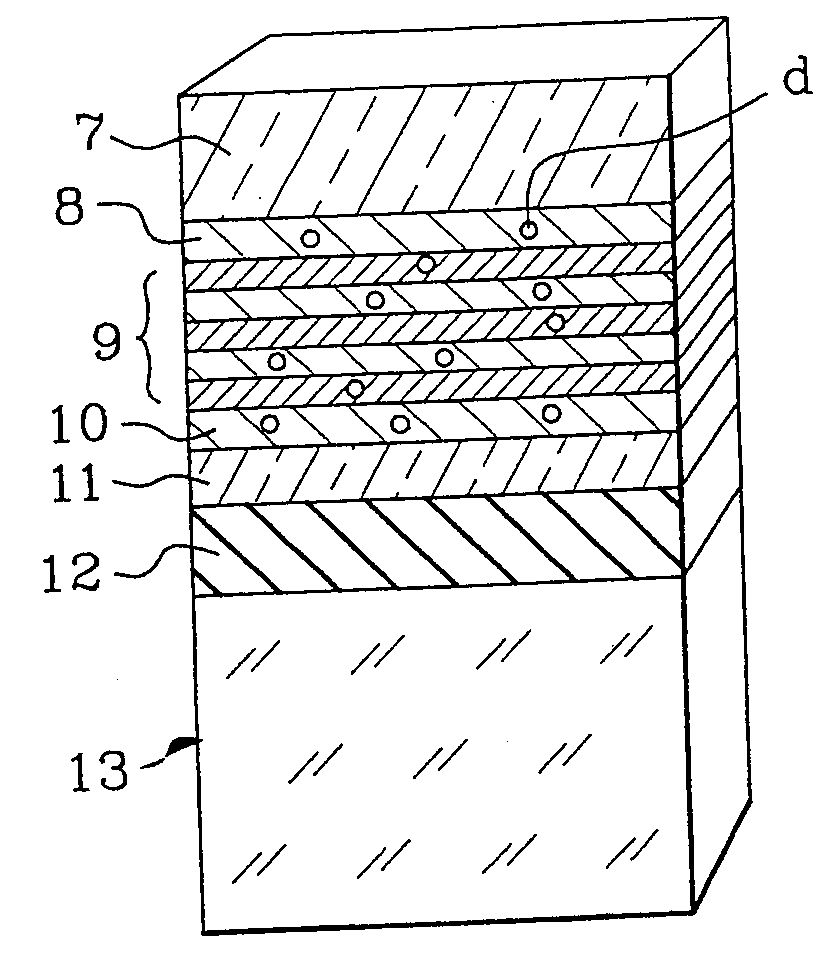
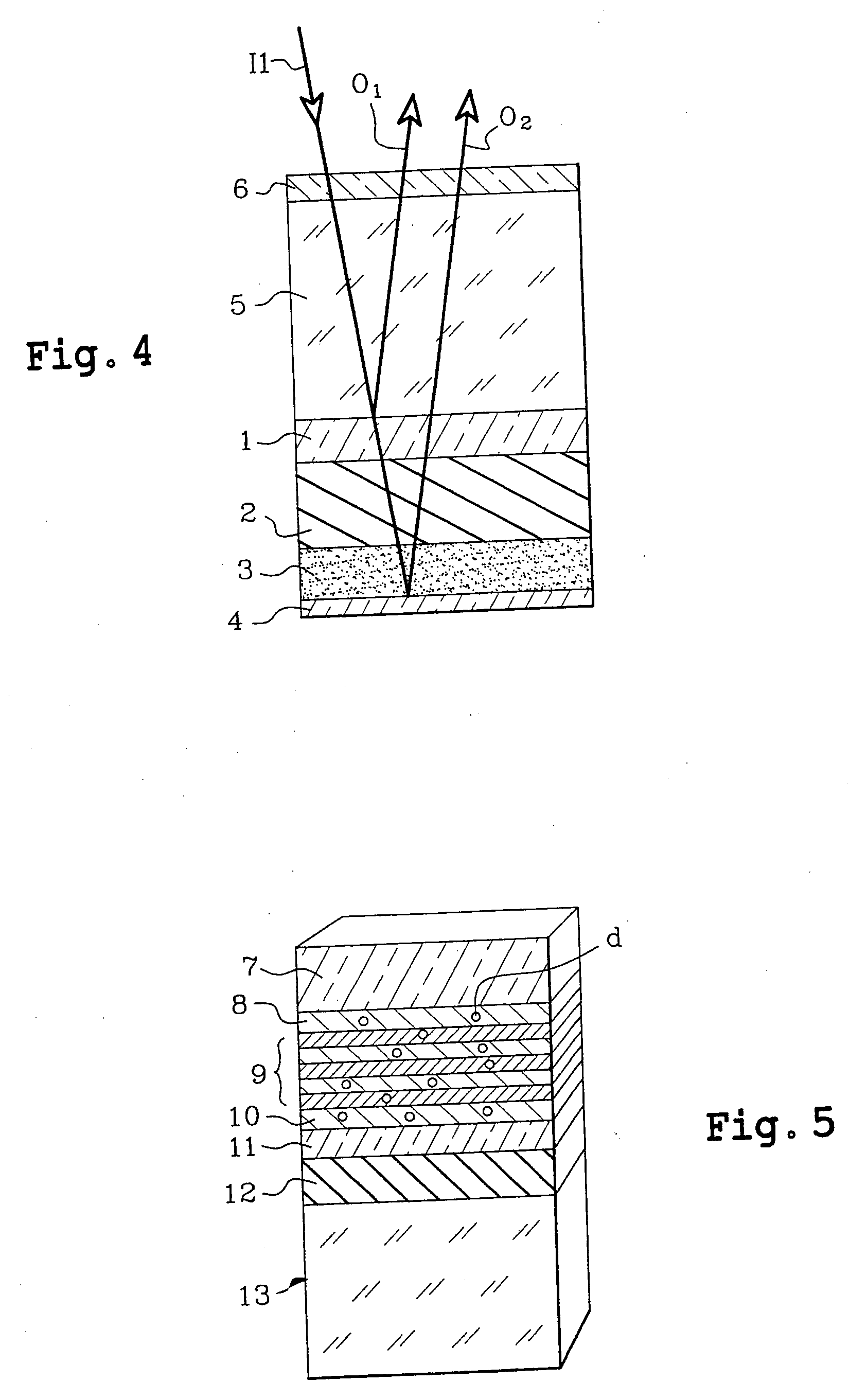
[0118]According to the second embodiment of the invention, the Bragg mirror is an epitaxy semiconductor mirror made during the growth stage of semiconductive layers on the aforementioned substrate 15. The semiconductive layers which were grown on the substrate 15 are thus successively the barrier layer 14, the Bragg mirror 7, the first phase layer 8, the absorbent structure 9 and the second phase layer 10. The Bragg mirror can then be composed, for example, of an alternation of InP and InGaAsP layers.

[0119]FIG. 14 represents a structure obtained following the epitaxial growth stage and FIG. 15 represents the irradiation stage of the thus obtained structure.

[0120]The irradiation stage follows the depositing stage of the rear mirror 11 and of the metallic layer 16 so as to obtain a structure such as represented in FIG. 16. The structure as represented in FIG. 16 is thus brought into contact with the structure as ...


PUM

PropertyMeasurementUnit
heat conductiveaaaaaaaaaa
metallicaaaaaaaaaa
crystalline defectsaaaaaaaaaa

Abstract

The invention relates to a saturable absorber component comprising an absorbent material located between a front mirror and a rear mirror as well as a method for manufacturing a saturable absorber component.The metallic rear mirror is a metallic buried mirror fixed via a welding joint on a heat conductive substrate.The invention applies to the field of high-rate optical transmission.

Description

CROSS REFERENCES[0001]This application is a Continuation of PCT application Ser. No. 10 / 499,659 filed Jun. 30, 2004 which is a National Stage of PCT / FR03 / 00169 filed Jan. 20, 2003 which claims priority to French Application No. 02 00756 filed Jan. 22, 2002, the entire contents of which are incorporated herein by reference.TECHNICAL FIELD AND PRIOR ART[0002]The invention relates to a saturable absorber component for the processing of digital optical signals as well as a method for manufacturing a saturable absorber component for the processing of digital optical signals.[0003]The component according to the invention has particularly advantageous applications in the field of high-rate optical transmission (all-optical signal regeneration for transatlantic communication, modulation contrast amplification, wavelength conversion, temporal demultiplexing optical sampling, etc.).[0004]Telecommunications and information technologies are currently booming. This growth in the exchange of info...

Claims


Application Information

Patent Timeline
Patent Type & Authority Applications(United States)
IPC IPC(8): B23K31/02B23K1/20G02F1/35
CPCG02F1/3523
Inventor OUDAR, JEAN-LOUISNELEP, CONSTANTINCHOUMANE, HOUTAI
Owner CENT NAT DE LA RECHERCHE SCI
Why Eureka
Try Eureka