Photoelectric conversion device and manufacturing method thereof

a technology manufacturing method, which is applied in the manufacture of final products, pv power plants, basic electric elements, etc., can solve the problems of reducing the productivity of photoelectric conversion device, the inability to efficiently use silicon semiconductors, and the inability to efficiently produce a sufficient number of photoelectric conversion devices. , to achieve the effect of reducing light loss, reducing production costs, and smooth flowing curren

Inactive Publication Date: 2009-05-21
SEMICON ENERGY LAB CO LTD
View PDF23 Cites 17 Cited by
  • Summary
  • Abstract
  • Description
  • Claims
  • Application Information

AI Technical Summary

Benefits of technology

[0019]The conductive clusters are located between the lower-layer unit cell and the upper-layer unit cell and forms an ohmic contact; thus, the conductive clusters have an effect of smoothly flowing current between the both unit cells. The conductive clusters are dispersed to be placed; thus, the conductive clusters have an effect of reducing loss of light entering the lower-layer unit cell from the upper-layer unit cell.
[0020]In the present invention, the single crystal semiconductor layer is obtained by separation of a surface layer of the single crystal semiconductor substrate. Since the single crystal semiconductor substrate can be reused, resources can be effectively used.

Problems solved by technology

Since the stacked-layer photoelectric conversion devices having a structure in which the different unit cells, which are the unit cell formed of a single crystal semiconductor and the unit cell formed of an amorphous semiconductor, are combined use a thick semiconductor substrate anyway, a challenge of efficiently using a silicon semiconductor cannot be achieved.
Therefore, a problem of decline in productivity of photoelectric conversion devices occurs.
After all, with a conventional technique, it is difficult to efficiently produce a sufficient number of photoelectric conversion devices which meet the demand by efficient use of limited materials.

Method used


Image

  • Photoelectric conversion device and manufacturing method thereof
  • Photoelectric conversion device and manufacturing method thereof
  • Photoelectric conversion device and manufacturing method thereof

Examples


embodiment mode 1

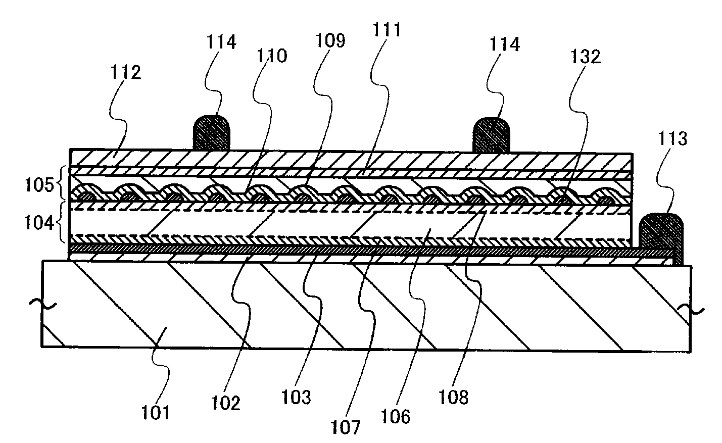
[0042]FIG. 1 is a plan view of a photoelectric conversion device 100 of this embodiment mode. This photoelectric conversion device 100 is provided with a first unit cell 104 and a second unit cell 105 which are fixed onto a supporting substrate 101. The first unit cell 104 and the second unit cell 105 include a semiconductor junction, and accordingly photoelectric conversion is performed by the semiconductor junction. Note that conductive clusters are dispersed between the first unit cell 104 and the second unit cell 105.

[0043]A first electrode is provided on the supporting substrate 101 side of the first unit cell 104, and a second electrode is provided on a surface side of the second unit cell 105. The first electrode is connected to a first auxiliary electrode 113. A second auxiliary electrode 114 is provided over the second electrode. The photoelectric conversion device 100 of this embodiment mode has a structure in which the first unit cell 104 and the second unit cell 105 are ...

embodiment mode 2

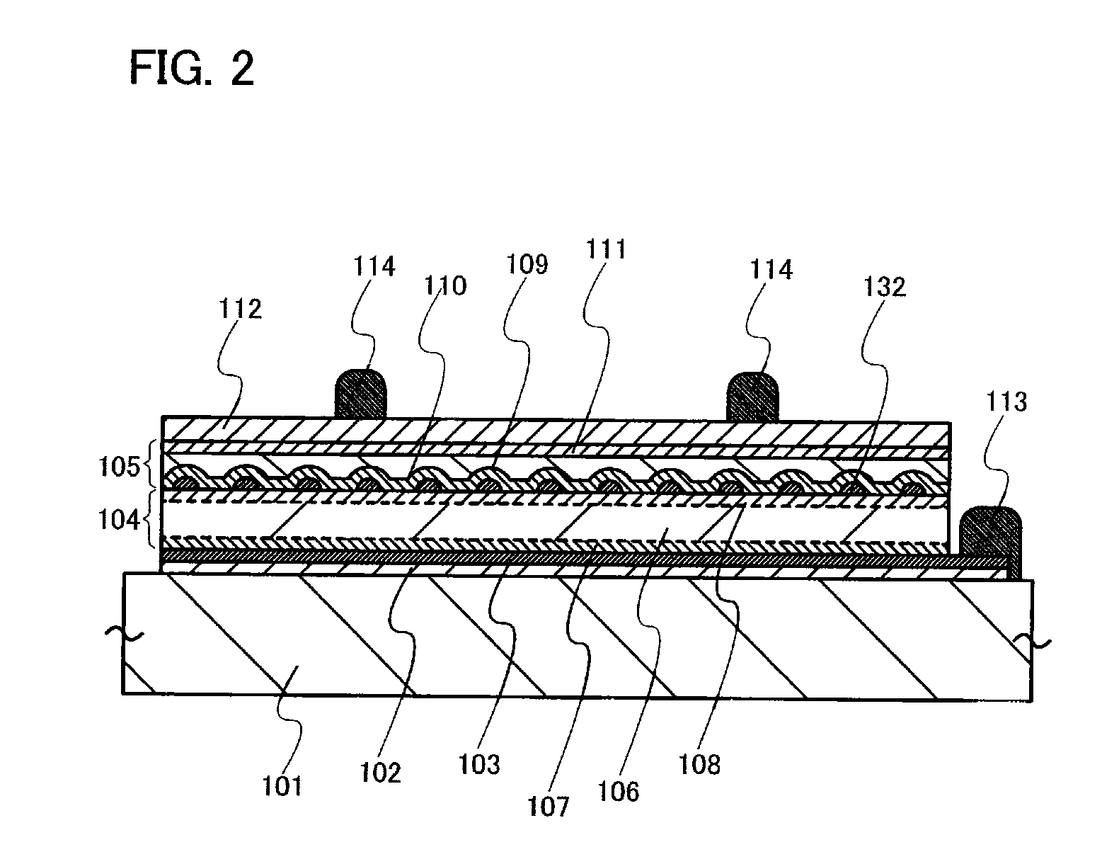
[0065]Next, a manufacturing method of the photoelectric conversion device 100 will be described on the premise of the case of FIG. 2 as a cross-sectional structure taken along the line A-B of FIG. 1.

[0066]A semiconductor substrate 119 shown in FIG. 5A is cut off from a circular single crystal semiconductor substrate to have a substantially quadrangular shape. Needless to say, the plane shape of the semiconductor substrate 119 is not particularly limited. However, in the case where a supporting substrate which forms a single crystal semiconductor layer is rectangular, the semiconductor substrate 119 is preferably substantially quadrangular. Single crystal silicon whose surface is mirror-polished is typically preferable for the semiconductor substrate 119. This is because the semiconductor substrate 119 is firmly attached to the supporting substrate with an insulating layer for bonding interposed therebetween. For example, a p-type single crystal silicon wafer with a resistance of app...

embodiment mode 3

[0101]In some cases, due to formation of the damaged layer 121, crystal defects remain at the surface of the single crystal semiconductor layer 106 which is exposed by separation of the semiconductor substrate 119 shown in FIG. 6B of Embodiment Mode 2. In that case, the surface part of the single crystal semiconductor layer 106 is preferably removed by etching. For the etching, dry etching or wet etching is performed. Further, in some cases, an uneven surface whose mean surface roughness (Ra) is 7 nm to 10 nm and whose largest difference in height between peak and valley (P-V) is 300 nm to 400 nm remains. Note that the “largest difference in height between peak and valley” in this specification refers to a difference in height between the peak and valley. The “peak” and the “valley” in this embodiment refer to a peak and a valley obtained by three-dimensional expansion of the “peak” and the “valley” defined by JIS B0101. The peak is represented by the highest part of the peaks of th...


PUM


Abstract

In order to form a metal thin film, a silicide film, or the like between an upper-layer unit cell and a lower-layer unit cell in stacked-layer photoelectric conversion devices, a step of forming the thin film is additionally needed. Therefore, a problem such as decline in productivity of the photoelectric conversion devices occurs. A first unit cell including a single crystal semiconductor layer with a thickness of 10 μm or less as a photoelectric conversion layer and a second unit cell including a non-single-crystal semiconductor layer as a photoelectric conversion layer, which is provided over the first unit cell, are at least included, and conductive clusters are dispersed between the unit cells. The conductive clusters are located between the lower-layer unit cell and the upper-layer unit cell to form an ohmic contact; thus, current flows between the both unit cells.

Description

BACKGROUND OF THE INVENTION[0001]1. Field of the Invention[0002]The present invention relates to a photoelectric conversion device in which a single crystal semiconductor or a polycrystalline semiconductor is used, and a photoelectric conversion device in which a plurality of photoelectric conversion elements are stacked.[0003]2. Description of the Related Art[0004]Photovoltaics is spreading as a clean and inexhaustible energy source. For photovoltaics, a photoelectric conversion device (also referred to as a “solar battery”) which converts photo energy into electrical energy with use of photoelectric characteristics of a semiconductor is used.[0005]The production of photoelectric conversion devices is increasing every year. For example, the worldwide production amount of solar batteries in 2005 is 1759 MW, which means drastic increase of 147% in comparison with the previous year. The photoelectric conversion devices using a crystal semiconductor is spreading worldwide, and photoele...

Claims


Application Information

Patent Timeline
Patent Type & Authority Applications(United States)
IPC IPC(8): H01L31/0376H01L31/18
CPCH01L31/02008H01L31/02021H01L31/03685H01L31/03762Y02E10/545H01L31/0725H01L31/1892Y02E10/544Y02E10/548H01L31/0687H01L2224/73253H01L2924/12044Y02P70/50H01L2924/00
Inventor YAMAZAKI, SHUNPEIARAI, YASUYUKI
Owner SEMICON ENERGY LAB CO LTD
Why Eureka
Try Eureka