
Semiconductor device comprising an image sensor, apparatus comprising such a semiconductor device and method of manufacturing such a semiconductor device

a semiconductor device and image sensor technology, which is applied in the direction of semiconductor devices, solid-state devices, television systems, etc., can solve the problems of index matching liquid similar locking problems, damage to the image sensor device, and inability to meet the requirements of image sensor operation, etc., to achieve the effect of cheap manufacturing and high yield

Inactive Publication Date: 2009-05-21
DALSA
View PDF12 Cites 3 Cited by
  • Summary
  • Abstract
  • Description
  • Claims
  • Application Information

AI Technical Summary

Benefits of technology

[0004]The invention has for its object inter alia to provide a semiconductor device of the kind mentioned in the opening paragraph, which can be manufactured with a high yield, and in a cheap manner.
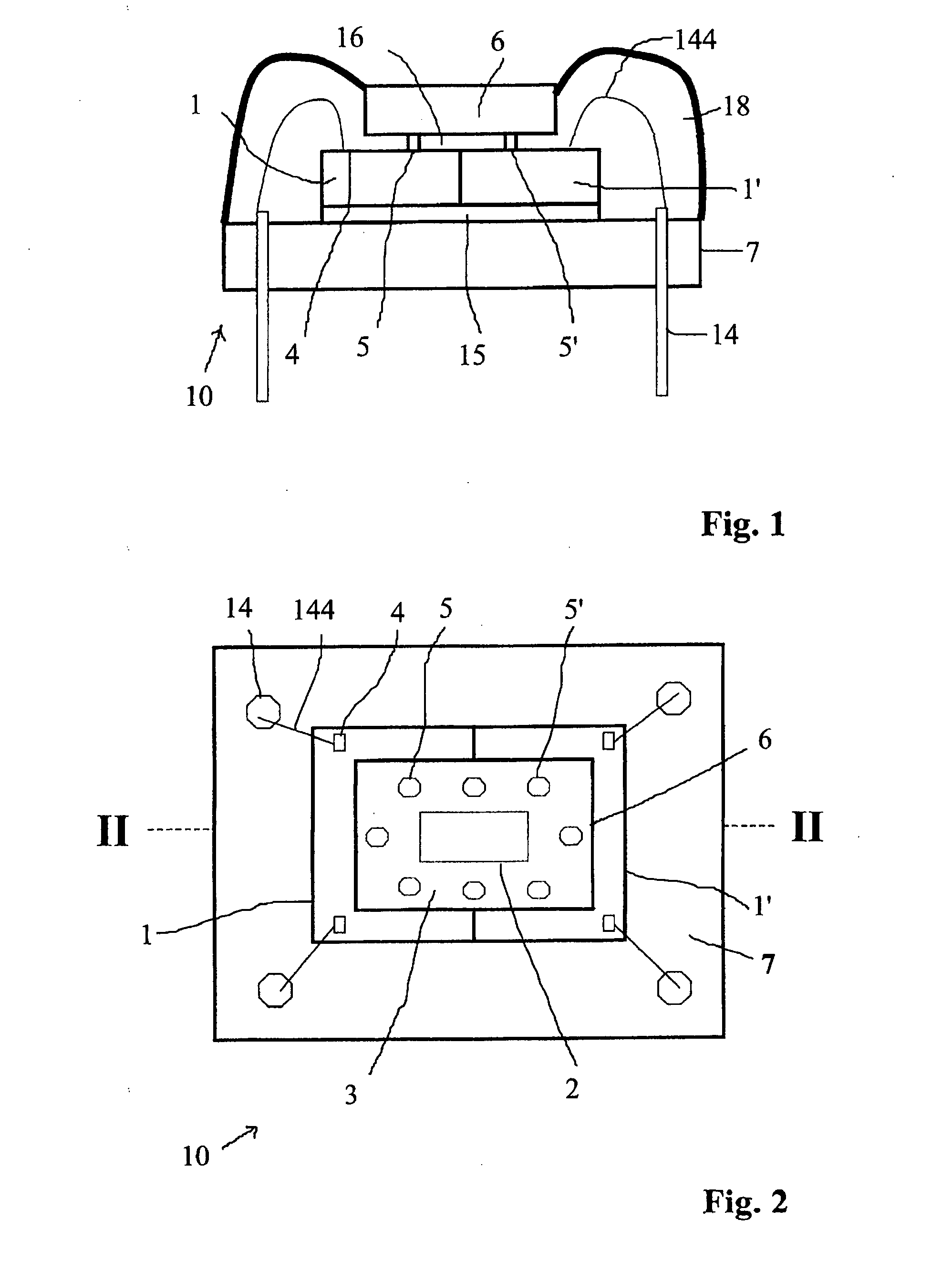
[0005]A semiconductor device according to the invention is characterized in that the spacer structure is an open structure allowing the atmosphere above the optically active part of the image sensor to contact the atmosphere outside the spacer structure. In this way, several problems are avoided that threaten the yield. Firstly, if now index-matching liquid is used within the spacer structure, out gassing of the material of the spacer structure may form a problem since such gasses are locked within the known spacer structure. Secondly, if such spacer structure is filled with an index matching liquid, similar locking problems can occur with said index matching liquid. By using an open spacer structure both gases and liquids (or gels) can leave the spacer structure and locking of such material is avoided.
[0006]A very simple way of obtaining the desired results is to provide an annular spacer structure like the prior art spacer structure with at least one interruption. Preferably however, such a ring structure is provided with a plurality of interruptions. In the most preferred embodiment the spacer structure comprises a plurality of dots. This offers very important additional advantages; apart from material saving an important manufacturing advantage is offered by the fact that the dots can be formed by a cheap and fast method like micro jetting.
[0007]Further surprising advantage are related to the specific nature of the device. The presence of a FOP easily damages the image sensor device reducing its manufacturing yield. If the spacer structure comprises dots, such damaging is much less likely to occur. The dots more easily cope with larger non-flatness both within the surface of the image sensor as in the surface of the FOP. In this way, the contact between image sensor and FOP is improved and the functioning of the dots as stress-releasing elements is improved as well. Due to a better stress-release damaging of the image sensor is avoided. In addition, the use of a plurality of dots offers a large freedom of design in the spacer structure. Due to a very limited size of the dots, they can be more easily and freely be positioned on the surface of the semiconductor body in the optically non-active part of the surface thereof, where however other passive semiconductor elements may be and in any case circuitry for operation and connection of the image sensor are present.
[0009]In a preferred embodiment the image sensor is positioned on and fixed to a carrier comprising further electrical connection areas that are electrically connected to the electrical connection areas of the image sensor. Preferably such a carrier is made of a metal like iron. This has the advantage of available cheap machining.
[0012]An important advantage of the embodiment in which the spacer structure comprises a plurality of dots is that these dots can be formed in a simple, cheap and fast manner. E.g. the technique of micro jetting may be advantageously be used for this purpose.

Problems solved by technology

Firstly, if now index-matching liquid is used within the spacer structure, out gassing of the material of the spacer structure may form a problem since such gasses are locked within the known spacer structure.
Secondly, if such spacer structure is filled with an index matching liquid, similar locking problems can occur with said index matching liquid.
The presence of a FOP easily damages the image sensor device reducing its manufacturing yield.

Method used


Image

  • Semiconductor device comprising an image sensor, apparatus comprising such a semiconductor device and method of manufacturing such a semiconductor device
  • Semiconductor device comprising an image sensor, apparatus comprising such a semiconductor device and method of manufacturing such a semiconductor device
  • Semiconductor device comprising an image sensor, apparatus comprising such a semiconductor device and method of manufacturing such a semiconductor device

Examples


Embodiment Construction

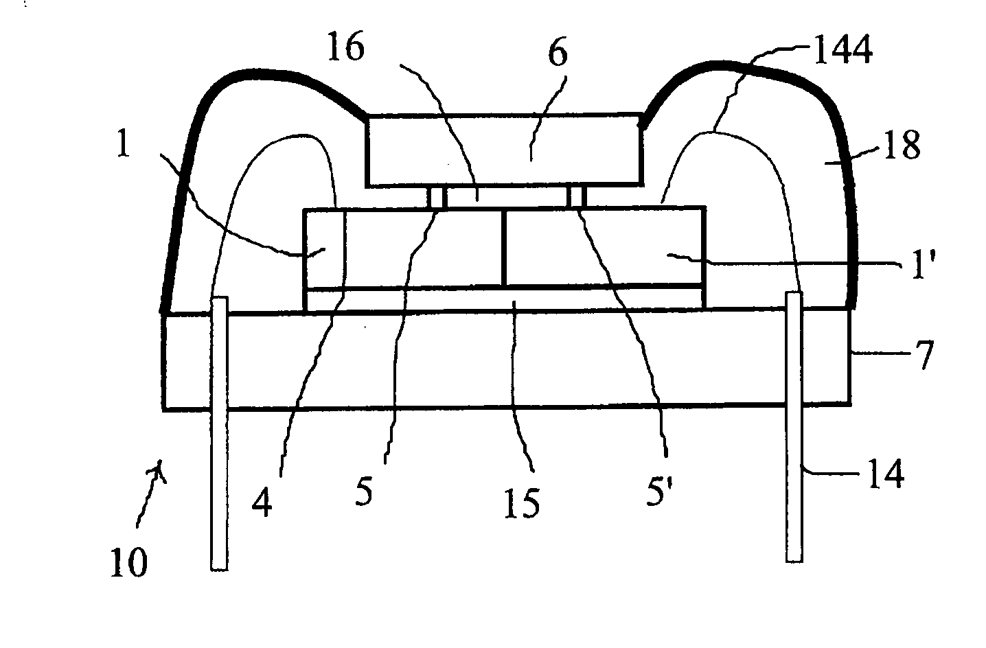
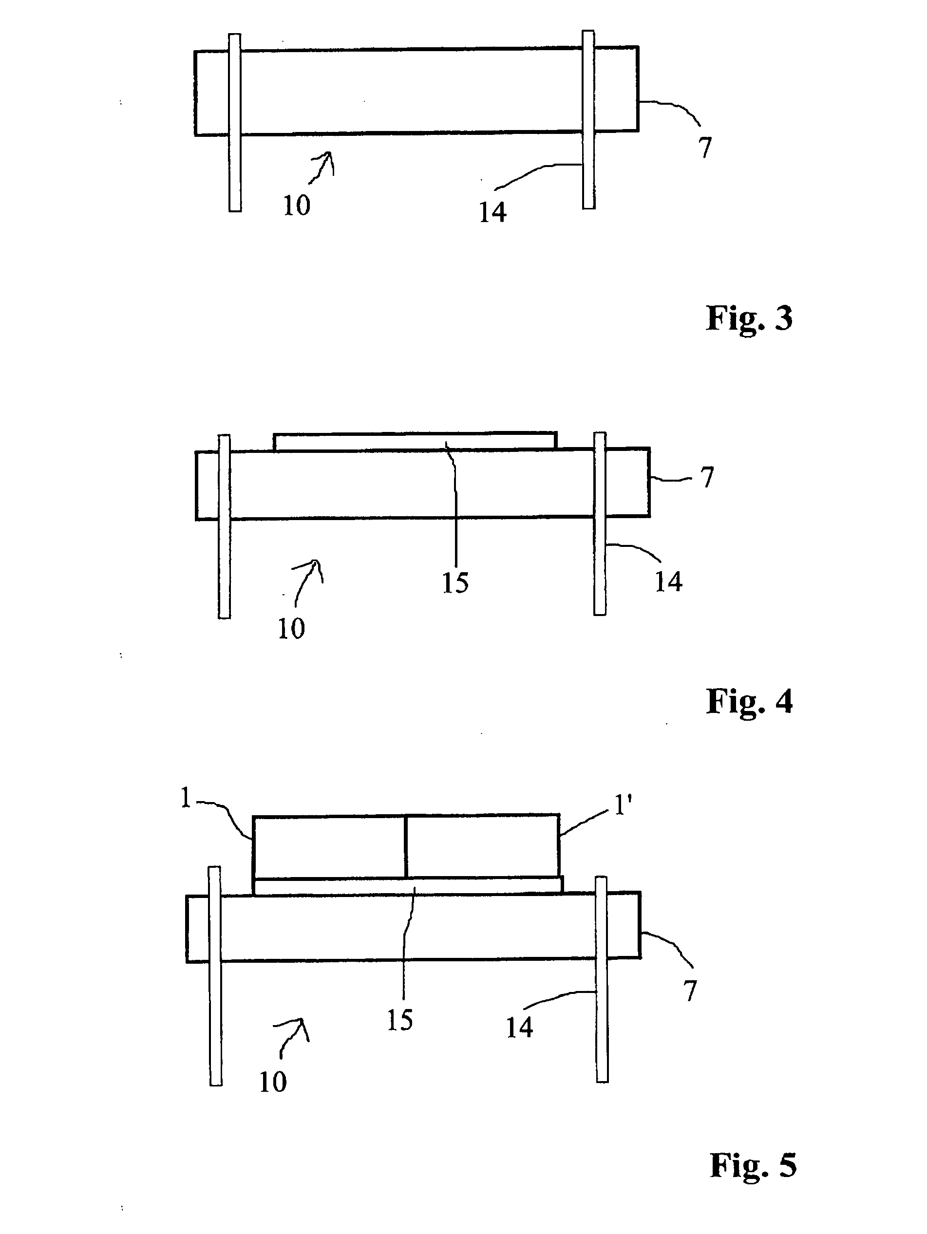
[0019]FIG. 1 shows a diagrammatic, cross-sectional view along the line II-II of a plan view as in FIG. 2 of an embodiment of a semiconductor device in accordance with the invention, and FIG. 2 diagrammatically shows a plan view of a relevant part of the embodiment of device shown in cross-section in FIG. 1. The device 10 comprises a carrier 7 made of Kovar (an Iron / Nickel alloy) which comprises electrically conducting pins 14, so-called PGA (=Pin Grid Array) pins, fixed in the carrier by means of a glass insulation. On the carrier 7 a die attach layer 15 is present by which a semiconductor body 1, in this example a plurality of semiconductor bodies 1, 1′, is attached to the carrier 7. The die attach layer 15 in this example is a layer of conductive epoxy and having a thickness of about 30-70 micron. The semiconductor bodies 1, 1′ comprise an image sensor and a further image sensor. These sensors are in this example of the CCD type and the size of the semiconductor bodies 1,1′ is abo...


PUM


Abstract

The invention relates to a semiconductor device comprising a semiconductor body in which an image sensor is formed and having a semiconductor body surface with an optically active part of the image sensor and a non-optically active part of the image sensor in which electrical connection areas of the image sensor are located, a spacer structure being present on the semiconductor body surface in the non-optically active part of the image sensor and an optical passive component being positioned on top of the spacer structure and above the image sensor and allowing radiation to impinge on the optically active part of the image sensor.According to the invention the spacer structure is an open structure allowing the atmosphere above the optically active part of the image sensor to contact the atmosphere outside the spacer structure. The spacer structure may comprise a ring provided with at least one interruption and positioned around the optically active part of the image sensor. Preferably, the spacer structure comprises a plurality of dots.

Description

BACKGROUND OF THE INVENTION[0001]The invention relates to a semiconductor device comprising a semiconductor body in which an image sensor is formed and having a semiconductor body surface with an optically active part of the image sensor and a non-optically active part of the image sensor in which electrical connection areas of the image sensor are located, a spacer structure being present on the semiconductor body surface in the non-optically active part of the image sensor and an optical passive component being positioned on top of the spacer structure and above the image sensor and allowing radiation to impinge on the optically active part of the image sensor. Such a semiconductor device may form a crucial component of a camera system. The image sensor may be either a CCD (=Charge Transfer Device) based device of the FT (=Frame Transfer) or so-called inter-line type. However, the sensor also may be a (C)MOS (=Complimentary Metal Oxide Semiconductor) device. The invention also rel...

Claims


Application Information

Patent Timeline
IPC IPC(8): H01L31/0203H01L31/18
CPCH01L27/14618H04N5/2253H01L27/14685H01L27/14625H01L2224/48091H01L2224/73265H04N23/54H01L2924/00014
Inventor VAN ARENDONK, ANTON PETRUS MARIAPANTEA, VICBENWELL, BRIAN WAYNE
Owner DALSA
Learn More