Oscillator, pll circuit, receiver and transmitter

a technology of oscillator and circuit, applied in the direction of pulse automatic control, oscillation generator, resonance circuit tuning, etc., can solve the problems of increased power consumption and large applicator scale, and achieve the effect of reducing the number of pads, reducing the size and manufacturing costs of the oscillator, and facilitating wiring

Inactive Publication Date: 2009-05-21
RICOH KK
View PDF7 Cites 6 Cited by
  • Summary
  • Abstract
  • Description
  • Claims
  • Application Information

AI Technical Summary

Benefits of technology

[0010]Also, it is desirable that all the components including the inductor are integrally formed on a semiconductor substrate using a CMOS process or a MOS process. Or it is desirable that all the components other than the inductor are integrally formed on a semiconductor substrate using a CMOS process or a MOS process. By producing the oscillator using these processes, the size and manufacturing costs of the oscillator can be reduced. In the case where all the components including the inductor are formed on the semiconductor substrate, the number of pads is reduced and the wiring is facilitated by eliminating an external component. On the other hand, in the case where the inductor is externally provided and the other components are formed on the semiconductor substrate, the low oscillation frequency and the high Q value can be easily realized.
[0011]A PLL circuit of the invention comprises the above mentioned oscillator within a phase locked loop. Specifically, the PLL circuit of the invention comprises the oscillator, a variable frequency divider for dividing an output signal of the oscillator at a frequency division ratio n settable from the outside, a phase comparator for making the phase comparison between an output signal of the variable frequency divider and a predetermined reference frequency signal, and a low pass filter for smoothing the output of the phase comparator to generate a control voltage as a control signal. The PLL circuit with the wide range of oscillation frequency can be easily realized by using the oscillator. In the oscillator, since the selected state is switched for each set of the variable capacitance element and the capacitor, there is uniform tendency of a change in the electrostatic capacities over the entire variable capacitance circuit to a variation amount ΔV of the control signal (control voltage) inputted into the variable capacitance elements, irrespective of the selected state. Accordingly, a lead-in time of the PLL circuit can be made almost constant without regard to the oscillation frequency.
[0012]Also, a receiver of the invention comprises a mixer for mixing an oscillation signal outputted from the PLL circuit and a reception signal received via an antenna, a filter for extracting a predetermined frequency component included in an output signal of the mixer, a demodulation circuit for performing a predetermined demodulating process for a signal after passing through the filter, and a control section for setting and changing the reception frequency by setting a frequency division ratio n of the variable frequency divider included in the PLL circuit. The receiver with the wide range of received frequency or band can be easily realized by using the PLL circuit having the oscillator. Also, the time required to switch the frequency can be prevented from varying with the frequency to be received by using the PLL circuit having almost constant lead-in time.
[0013]Also, a transmitter of the invention comprises a transmission circuit for transmitting a transmission signal from an antenna by generating the transmission signal with an oscillation signal outputted from the PLL circuit as a carrier, and a control section for setting and changing the transmission frequency by setting a frequency division ratio n of the variable frequency divider included in the PLL circuit. The transmitter with the wide range of transmission frequency or transmission band can be easily realized by using the PLL circuit having the oscillator. Also, the time required to switch the frequency can be prevented from varying with the transmission frequency to be switched by using the PLL circuit having almost constant lead-in time.

Problems solved by technology

By the way, it was required that a plurality of VCOs having the same basic configuration are provided on the IC in the receiver as disclosed in Japanese Patent Application Laid-Open No. 2003-110425, whereby there was a problem that the apparatus scale was large.
Further, in the case where the plurality of oscillators are selectively used, it is required to send a current through the stand-by oscillators other than the selected oscillator which is operating at that time, in consideration of the stability of operation immediately after switching, whereby the power consumption is increased.

Method used


Image

  • Oscillator, pll circuit, receiver and transmitter
  • Oscillator, pll circuit, receiver and transmitter
  • Oscillator, pll circuit, receiver and transmitter

Examples


Embodiment Construction

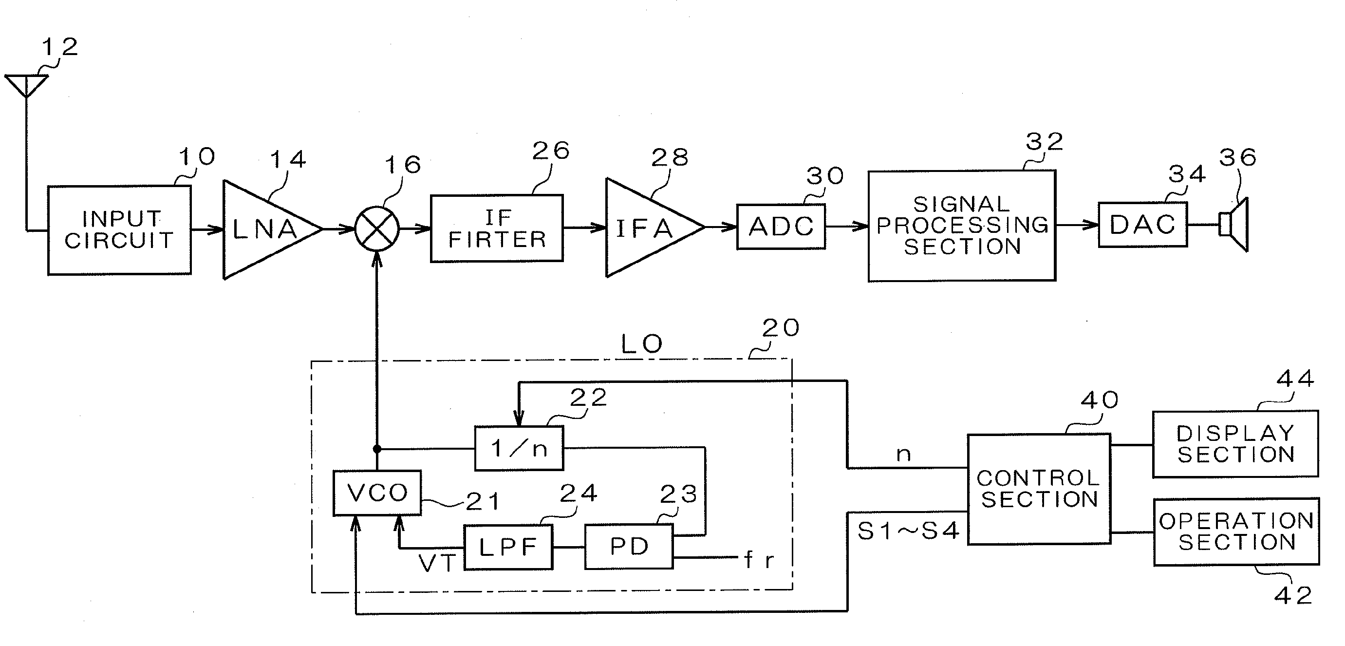
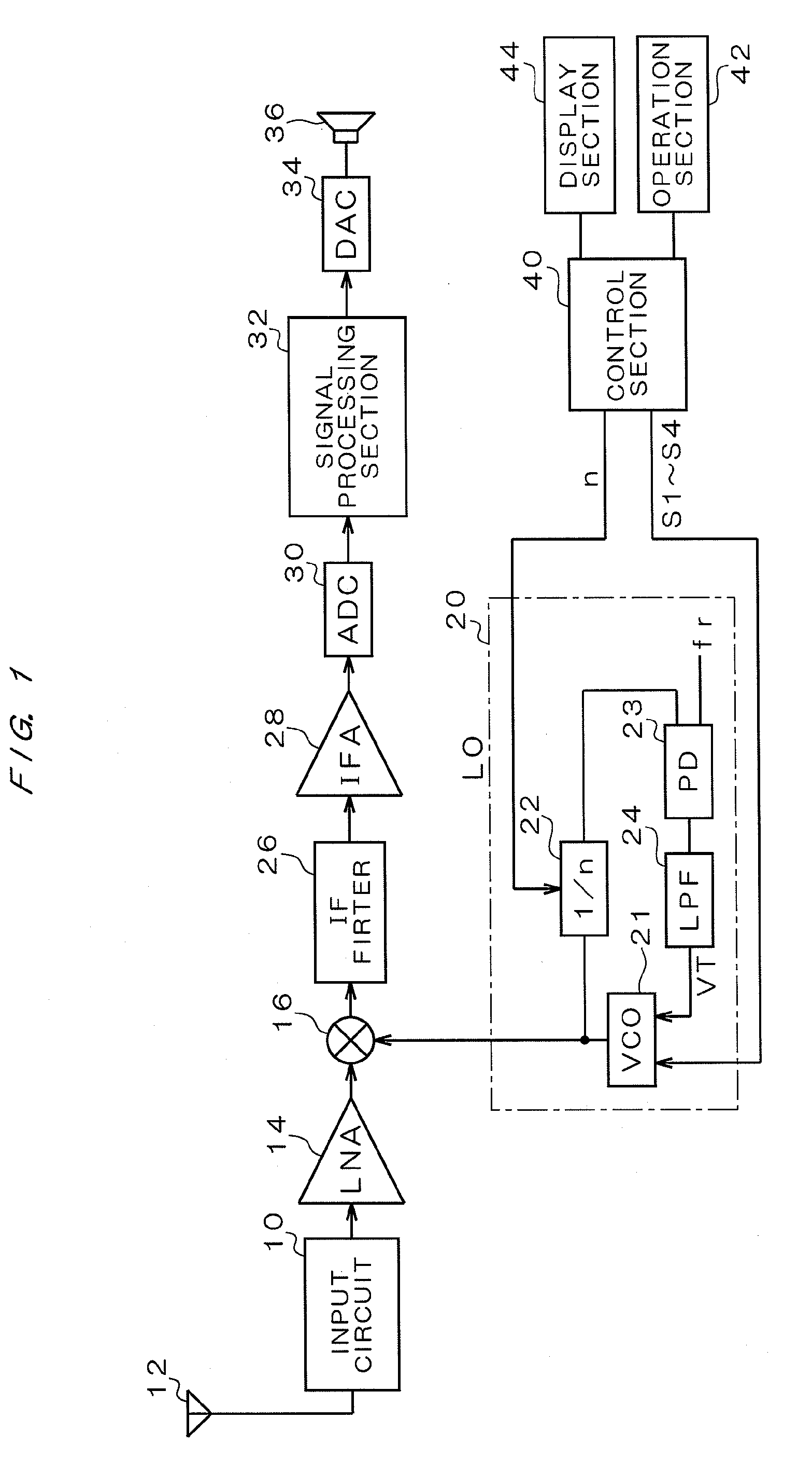
[0040]A receiver according to one embodiment of the present invention will be described below in detail. FIG. 1 is a diagram showing the basic configuration of the receiver according to one embodiment. The receiver of this embodiment comprises an input circuit 10, a low noise amplifier (LNA) 14, a mixer 16, a local oscillator (LO) 20, an intermediate frequency filter (IF filter) 26, an intermediate frequency amplifier (IFA) 28, an analog-digital converter (ADC) 30, a signal processing section 32, a digital-analog converter (DAC) 34, a speaker 36, a control section 40, an operation section 42, and a display section 44, as shown in FIG. 1. This receiver receives an FM broadcast wave, for an example, but has the same basic configuration when receiving an AM broadcast wave or television broadcast wave. Also, in this receiver, most of the components except for the antenna 12 and speaker 36 or a few other parts (e.g., a crystal oscillator required for generating the operation clock of the...


PUM


Abstract

An oscillator, a PLL circuit, a receiver and a transmitter that allow the circuit scale to be reduced and that are suitable for integration. The electrostatic capacities of variable capacitance circuits 230, 230A are made variable, thereby varying the oscillation frequency of a voltage controlled oscillator 21. The variable capacitance circuit 230 comprises a plurality of variable capacitance elements 60-64 the electrostatic capacities of which can be continuously varied by use of a control signal; a plurality of capacitors 50-54 which are associated with the respective variable capacitance elements and the electrostatic capacities of which are fixed; and a plurality of switches 71-74, 81-84 that individually switch combinational circuits, each of which comprises one of the plurality of variable capacitance elements 60-64 and a respective associated one of the plurality of capacitors 50-54, for selective connections.

Description

TECHNICAL FIELD[0001]The present invention relates to an oscillator in which the oscillation frequency is set according to a control voltage, a PLL circuit, a receiver and a transmitter.BACKGROUND ART[0002]To realize the reduced size and lower costs of a receiver, a technology for making a front-end module including a VCO (Voltage Controlled Oscillator) in chip form is well known (for example, see Japanese Patent Application Laid-Open No. 2003-110425). The oscillation frequency of the VCO is controlled by varying a voltage applied to a variable capacitance element included in the VCO, but because a capacity change of the variable capacitance element that can be implemented on the TC is small, a plurality of VCOs are provided to cover a wide variable range of frequencies in the receiver as disclosed in Japanese Patent Application Laid-Open No. 2003-110425 (pages 6 to 16, FIGS. 1 to 46).DISCLOSURE OF THE INVENTION[0003]By the way, it was required that a plurality of VCOs having the sa...

Claims


Application Information

Patent Timeline
Patent Type & Authority Applications(United States)
IPC IPC(8): H03L7/08
CPCH03B2200/005H03B2201/025H03J2200/10H03L7/099H03B5/124H04B1/28H03B5/1228H03B5/1212H03B5/1265H03L7/18H03B5/24H04B1/26
Inventor MIYAGI, HIROSHI
Owner RICOH KK
Why Eureka
Try Eureka