
Semiconductor integrated circuit device

Inactive Publication Date: 2009-05-21
RENESAS ELECTRONICS CORP
View PDF6 Cites 10 Cited by
  • Summary
  • Abstract
  • Description
  • Claims
  • Application Information

AI Technical Summary

Benefits of technology

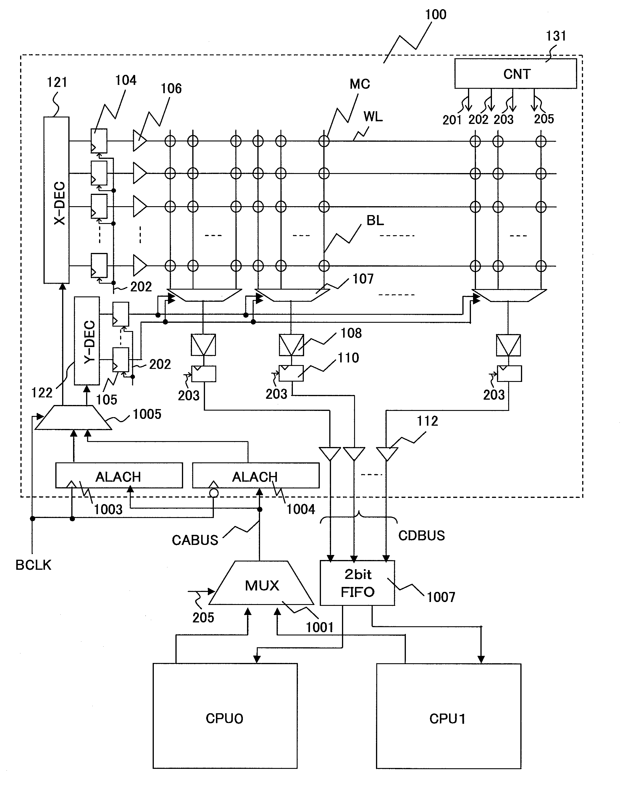
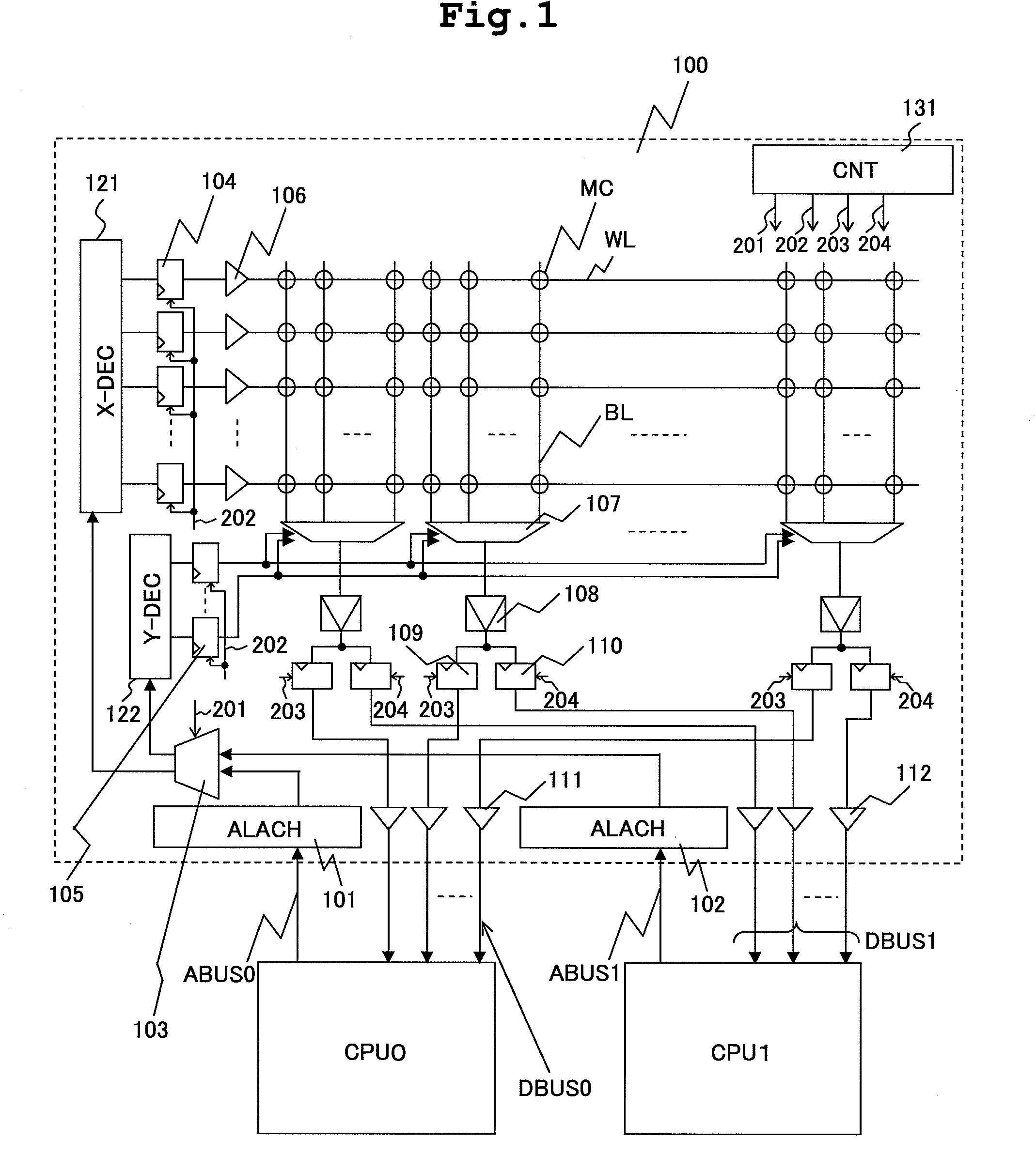
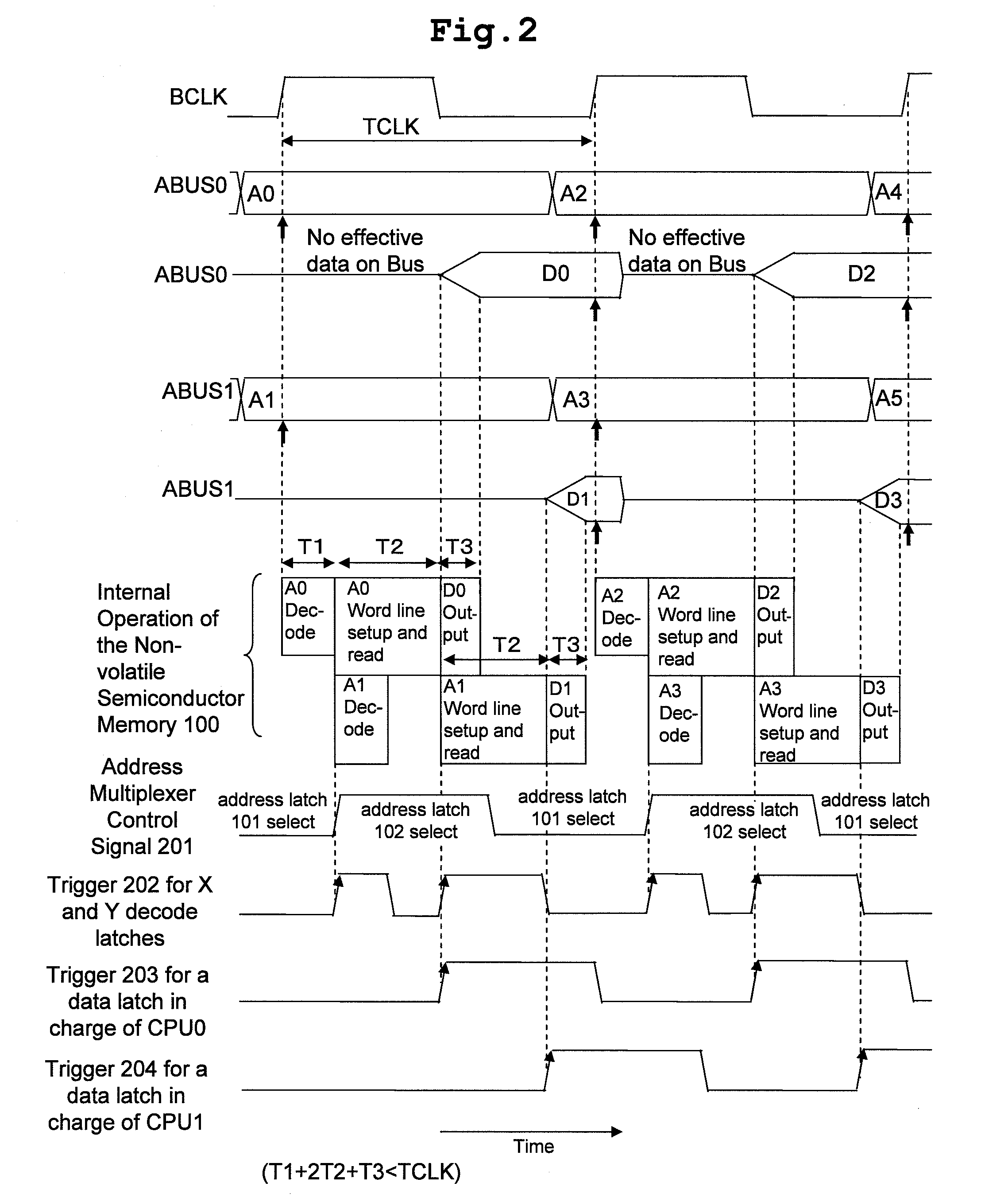
[0016]In a post stage subsequent to the X decoder, a first latch which can hold an output signal of the X decoder and transfer the signal to the word driver is disposed. In the post stage subsequent to the Y decoder, a second latch which can hold an output signal of the Y decoder and transfer the signal to the column multiplexer is disposed. In the post stage subsequent to the sense amplifier, a third latch which can hold an output signal of the sense amplifier and transfer the signal to the output buffer is disposed. The structure as stated above makes it possible to pipeline-control a series of processes for reading data stored in the non-volatile semiconductor memory. In addition, it enables low-latency access even with access requests from CPUs conflicting.
[0021]The structure as described above makes it possible to pipeline-control a series of processes for reading data stored in the non-volatile semiconductor memory. This enables low-latency access even with access requests from CPUs conflicting.

Problems solved by technology

Therefore, it is considered that the finite memory capacity cannot be leveraged effectively, and an unused memory region tends to arise.
In contrast, as for shared memory system that a memory is shared by CPUs, it is conceivable that one memory region can be used effectively, however the conflict between accesses by CPUs to the shared memory, and the conflict of data transfer on a bus tend to occur.
Therefore, the increase in the latency in connection with data transfer inside a chip can cause the degradation of performance.
Now, as to a multi processor system, during execution of a system setup initial diagnosis in accordance with an initial diagnosis program (hereinafter referred to as “firmware” or its abbreviation “FW”), CPUs on two or more modules read a diagnosis program on a non-volatile memory common to the CPUs, which is a diagnosis module, concurrently, and thus the system performance is deteriorated.

Method used


Image

  • Semiconductor integrated circuit device
  • Semiconductor integrated circuit device
  • Semiconductor integrated circuit device

Examples


first embodiment

[0056]FIG. 18 shows a multi processor system, as an example of a semiconductor integrated circuit device in accordance with the invention.

[0057]Although no special restriction is intended, the multi processor system 10 shown in FIG. 18 is formed on a single semiconductor substrate, such as single crystal silicon substrate, by the well-known techniques of manufacturing semiconductor integrated circuits.

[0058]The multi processor system 10 shown in FIG. 18 has processors CPU0 and CPU1, an input / output (I / O) circuit 200 and a non-volatile semiconductor memory (MEM) 100 connected by a system bus BUS so that they can exchange signal with one another. However, no special restriction is intended with respect to this. The input / output circuit 200 is connected to two or more peripheral circuits (PER) 300 through a local bus 400. The peripheral circuits 300 include an A / D converter for converting an input analog signal into a digital signal, and a timer for measuring time. The non-volatile sem...

second embodiment

[0089]FIG. 3 shows an example of another structure of the multi processor system 10. The non-volatile semiconductor memory 100 shown in FIG. 3 differs from that shown in FIG. 1 significantly in that first-in first-out buffers (2-bit FIFO) 303 and 304 which take a 2-bit structure of address bus ABUS and data bus DBUS are provided. The operations of the 2-bit FIFOs 303 and 304 are controlled in accordance with a 2-bit FIFO trigger signal 401 produced by the control circuit 131.

[0090]The first embodiment requires that the read from the non-volatile semiconductor memory should meet the following condition expressed using the clock cycle TCLK defined as shown in FIG. 2 and the time lengths T1 to T3: T1+2T2+T3<TCLK”. However, the difference in speed between CPUs and memories tends to expand year by year in general. Therefore, it is difficult to meet the condition as described above except when a very high performance is not required and the CPUs' clocks are at most tens of megahertz.

[0091...

third embodiment

[0102]FIG. 5 shows an example of another structure of the multi processor system 10.

[0103]The multi processor system shown in FIG. 5 differs from that shown in FIG. 3 in that the read latency is improved by cache memories (CMEM) 501 and 502 disposed between the processors CPU0 and CPU1 and the non-volatile semiconductor memory 100.

[0104]The multi processor system in accordance with the second embodiment offers a sufficient throughput because an address can be accepted to output data every clock cycle. However, in the multi processor system, the read latency is 2TCLK, which has the effect of reducing the latency at the time of occurrence of read conflict between two CPUs by half, however cannot shorten the read latency per read to 1TCLK.

[0105]Hence, low-latency cache memories 501 and 502 are placed between the processors CPU0 and CPU1 and the non-volatile semiconductor memory 100 as shown in FIG. 5. The cache memories 501 and 502 each offer a latency of 1TCLK and have a performance t...


PUM


Abstract

The semiconductor integrated circuit device includes: a first latch which can hold an output signal of the X decoder and transfer the signal to the word driver in a post stage subsequent to the X decoder; a second latch which can hold an output signal of the Y decoder and transfer the signal to the column multiplexer in the post stage subsequent to the Y decoder; and a third latch which can hold an output signal of the sense amplifier and transfer the signal to the output buffer in the post stage subsequent to the sense amplifier. The structure makes it possible to pipeline-control a series of processes for reading data stored in the non-volatile semiconductor memory, and enables low-latency access even with access requests from CPUs conflicting.

Description

CLAIM OF PRIORITY[0001]The Present application claims priority from Japanese application JP 2007-297479 filed on Nov. 16, 2007, the content of which is hereby incorporated by reference into this application.DESCRIPTION OF THE RELATED ARTField of the Invention[0002]The present invention relates to a semiconductor integrated circuit including a non-volatile semiconductor memory accessible for CPUs (Central Processing Units), and more particularly a technique useful e.g. in application to a multi processor system.BACKGROUND OF THE INVENTION[0003]In The fields of system LSIs and microcontrollers, the introduction of a multi-core structure that a plurality of CPUs are implemented in a chip has been progressing for the purpose of simultaneously achieving the suppression of increase in power consumption stemming from the rise in the frequency of clocks, and the enhancement of the performance. In parallel with such trend, in design of system LSIs, we are pressed with the urgent need to sele...

Claims


Application Information

Patent Timeline
IPC IPC(8): G11C7/00G11C8/08G11C8/00G11C7/06
CPCG11C7/1039G11C16/26G11C7/1075
Inventor KAJIYAMA, SHINYASHINAGAWA, YUTAKAMIZUNO, MAKOTOKASAI, HIDEOWATANABE, TAKAOTAKEMURA, RIICHIROSEKIGUCHI, TOMONORI
Owner RENESAS ELECTRONICS CORP
Learn More