Check patentability & draft patents in minutes with Patsnap Eureka AI!

Structure for SRAM voltage control for improved operational margins

Active Publication Date: 2009-05-21
INFINEON TECH LLC
View PDF28 Cites 1 Cited by
  • Summary
  • Abstract
  • Description
  • Claims
  • Application Information

AI Technical Summary

Benefits of technology

[0012]According to embodiments of the invention described herein, a design structure embodied in a machine readable medium used in a design process includes a static random access memory (“SRAM”) which includes a plurality of SRAM cells arranged in an array. The array includes a plurality of rows and a plurality of columns. The SRAM includes voltage control circuits corresponding to respective ones of the plurality of columns of the array, each coupled to an output of a power supply. Each voltage control circuit temporarily reduces a voltage provided to power supply inputs of a plurality of SRAM cells that belong to a selected column of columns of the SRAM. The power supply voltage to the selected column is reduced during a write operation in which a bit is written to one of the SRAM cells belonging to the selected column.
[0013]In addition, in one or more of the embodiments described below, an NFET is used to actively pull down the power supply voltage from the nominal level Vdd to a lowered level Vdda, a process which in some instances can be made to occur faster than simply allowing the power supply voltage level to float down to a certain level. In addition, timing is preferably controlled so that the power supply voltage is reduced, and write values appear on the bitlines before the wordline is activated. In this way, maximum use is made of the limited duration duty cycle of the wordline. These things make it possible to scale the SRAM cell further while maintaining or increasing the sigma value. With higher sigma values of ADM and WRM, larger sizes of caches and buffers can be accommodated without increasing the likelihood that an error will occur.
[0014]In accordance with one or more embodiments of the invention, design structure including an SRAM is provided which includes NFETs as passgates of the cells therein. For the same size and similar processes used to manufacture NFETs and PFETs, NFETs produce higher on-current than PFETs. This occurs because of the higher mobility of electrons, the dominant charge carriers in NFETs, as compared to the mobility of holes, the dominant charge carriers in PFETs. Therefore, when the size of NFETs and PFETs and their manufacturing processes are about the same NFET passgates permit the SRAM cell to be written more quickly than PFET passgates. Thus, for the same size of structure with an SRAM cell and the same ADM value, a higher WRM value is generally achieved using NFET passgates than when using PFET pass-gates. Conversely, for same WRM value and ADM value, smaller SRAM cell size can be achieved using NFET passgates than can be achieved using PFET pass-gates.

Problems solved by technology

The increased variability of the threshold voltage of the FETs of cells of an SRAM and the reduced power supply voltage level make it harder to guarantee that certain margins of error are maintained during operation of the SRAM.
Such margins of error have a direct bearing on the SRAM's ability to maintain the integrity of the data stored therein.
Clearly, there is a requirement that an extremely miniscule amount of such errors occur during operation of an SRAM.
Such “half” selected cells are more susceptible to disturbance during access to the cells within the SRAM because such cells are frequently subject to potential disturbance during such accesses at times when they are not being accessed.
Another margin of error that must be satisfied is the ability to write the state of bit to an SRAM cell, given the strength of the bitline signals supplied to the SRAM cell and the time allotted to do so.
If the SRAM cell fails to be written with the bit that is provided thereto, data integrity is impacted.
The scaling of one or more voltages supplied to each SRAM cell of the SRAM array for each succeeding generation of SRAMs only increases the difficulty of achieving a desired ADM and desired WRM.
However, such approach potentially worsens WRM.
In an SRAM, the available amount of drive current within each SRAM cell is already limited because of the scaling of the voltage.
As a result, raising the threshold voltages of the NFET and PFET make the NFET weaker and the PFET stronger.
While the SRAM cell becomes more stable under such conditions, writing each SRAM cell becomes more difficult than before.
As transistor sizes are scaled further downward in future generations of SRAMs, it becomes more difficult to achieve desirable sigma values on both ADM and WRM over the range of temperatures in which SRAMs (and processors which incorporate them) are required to operate.

Method used


Image

  • Structure for SRAM voltage control for improved operational margins
  • Structure for SRAM voltage control for improved operational margins
  • Structure for SRAM voltage control for improved operational margins

Examples


Embodiment Construction

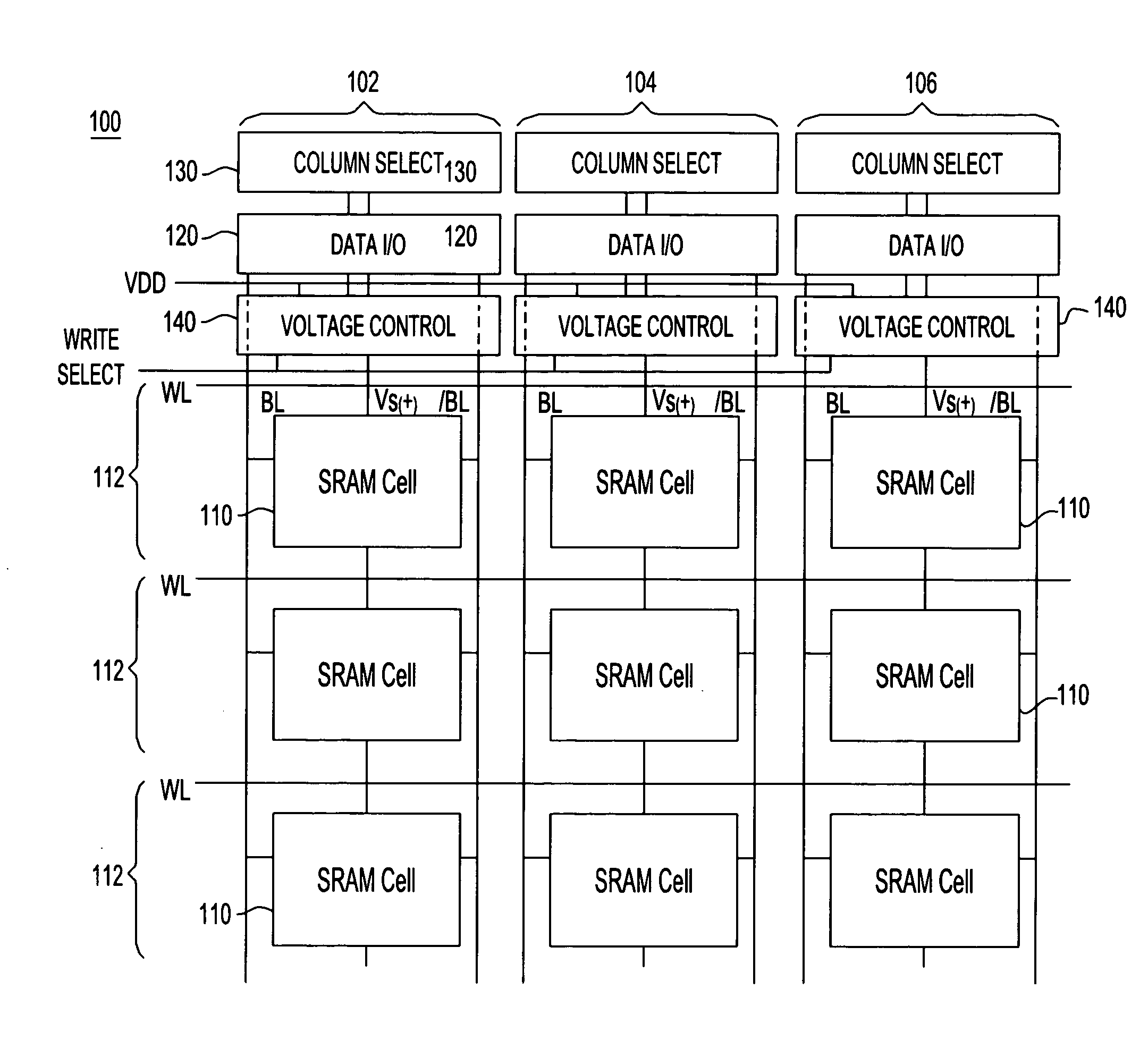
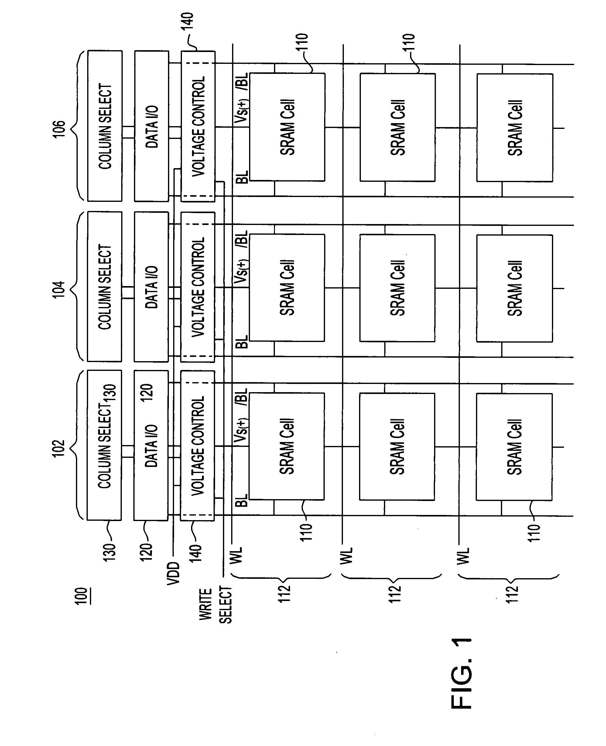
[0025]U.S. patent application Ser. No. 11 / 164,556 filed Nov. 29, 2005 to Wayne F. Ellis et al. entitled “SRAM Voltage Control for Improved Operational Margins” is incorporated by reference herein. FIG. 1 is a block and schematic diagram illustrating a static random access memory (SRAM) 100 in accordance with an embodiment of the invention. The SRAM 100 can be a stand-alone SRAM on a dedicated chip containing only one or more such SRAMs 100, or be incorporated into a chip having one or more additional functions, such as incorporated into a chip on which a processor or network interface is provided, for example.

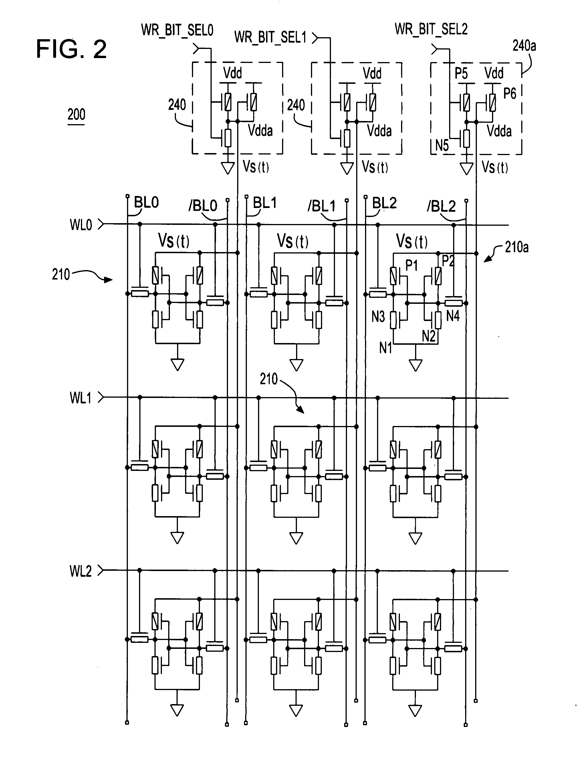
[0026]As illustrated in FIG. 1, the SRAM includes a plurality of storage cells 110, each storage cell operable to store a data bit and to provide read access and write access thereto when power is supplied to the SRAM 100 during normal operation. The SRAM 100 typically includes many such cells, ranging from several thousand cells per SRAM to many millions of cells. Within the S...


PUM


Abstract

A design structure including a static random access memory (“SRAM”) is provided which includes a plurality of SRAM cells arranged in an array. The array includes a plurality of rows and a plurality of columns. The SRAM includes voltage control circuits corresponding to respective ones of the plurality of columns of the array, each coupled to an output of a power supply. Each voltage control circuit temporarily reduces a voltage provided to power supply inputs of a plurality of SRAM cells that belong to a selected column of columns of the SRAM. The power supply voltage to the selected column is reduced during a write operation in which a bit is written to one of the SRAM cells belonging to the selected column.

Description

BACKGROUND OF THE INVENTION[0001]An important factor that The present invention relates to static random access memories (“SRAMs”), and more particularly to SRAMs having circuits for altering a voltage level supplied thereto. In addition, aspects of the invention relate to methods of operating an SRAM in which a voltage level supplied thereto is altered.[0002]SRAMs are uniquely suited to the functions they serve within processors and other devices for storage of data to which fast (low cycle time) and ready (low latency) access is desired. Certain types of storage within processors are almost always implemented using SRAMs, such as cache memories, control stores, buffer memories, instruction pipelines and data pipelines including input output interfaces and buffers for direct memory access (“DMA”) interfaces. In addition, certain storage used for communication interfaces, e.g., network adapter buffers and so on, also utilize SRAMs for speed and low latency. Since SRAMs are frequentl...

Claims


Application Information

Patent Timeline
IPC IPC(8): G11C5/14
CPCG11C11/413G11C5/14
Inventor ELLIS, WAYNE F.MANN, RANDY W.WAGER, DAVID J.WONG, ROBERT C.
Owner INFINEON TECH LLC
Features
  • R&D
  • Intellectual Property
  • Life Sciences
  • Materials
  • Tech Scout
  • Unparalleled Data Quality
  • Higher Quality Content
  • 60% Fewer Hallucinations
Learn More