
Processing apparatus

a technology of processing apparatus and processing vessel, which is applied in the direction of coating, chemical vapor deposition coating, electric discharge tube, etc., can solve the problems of high probability, difficult to remove unnecessary film adhering thereto at a low temperature, and high temperature, so as to improve the energy efficiency involved in heating and/or cooling the processing vessel

Inactive Publication Date: 2009-05-28
TOKYO ELECTRON LTD
View PDF11 Cites 22 Cited by
  • Summary
  • Abstract
  • Description
  • Claims
  • Application Information

AI Technical Summary

Benefits of technology

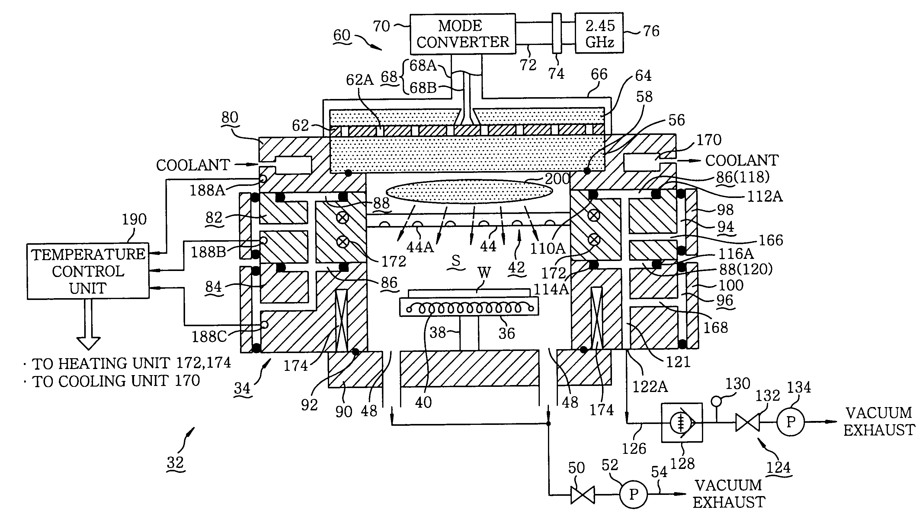
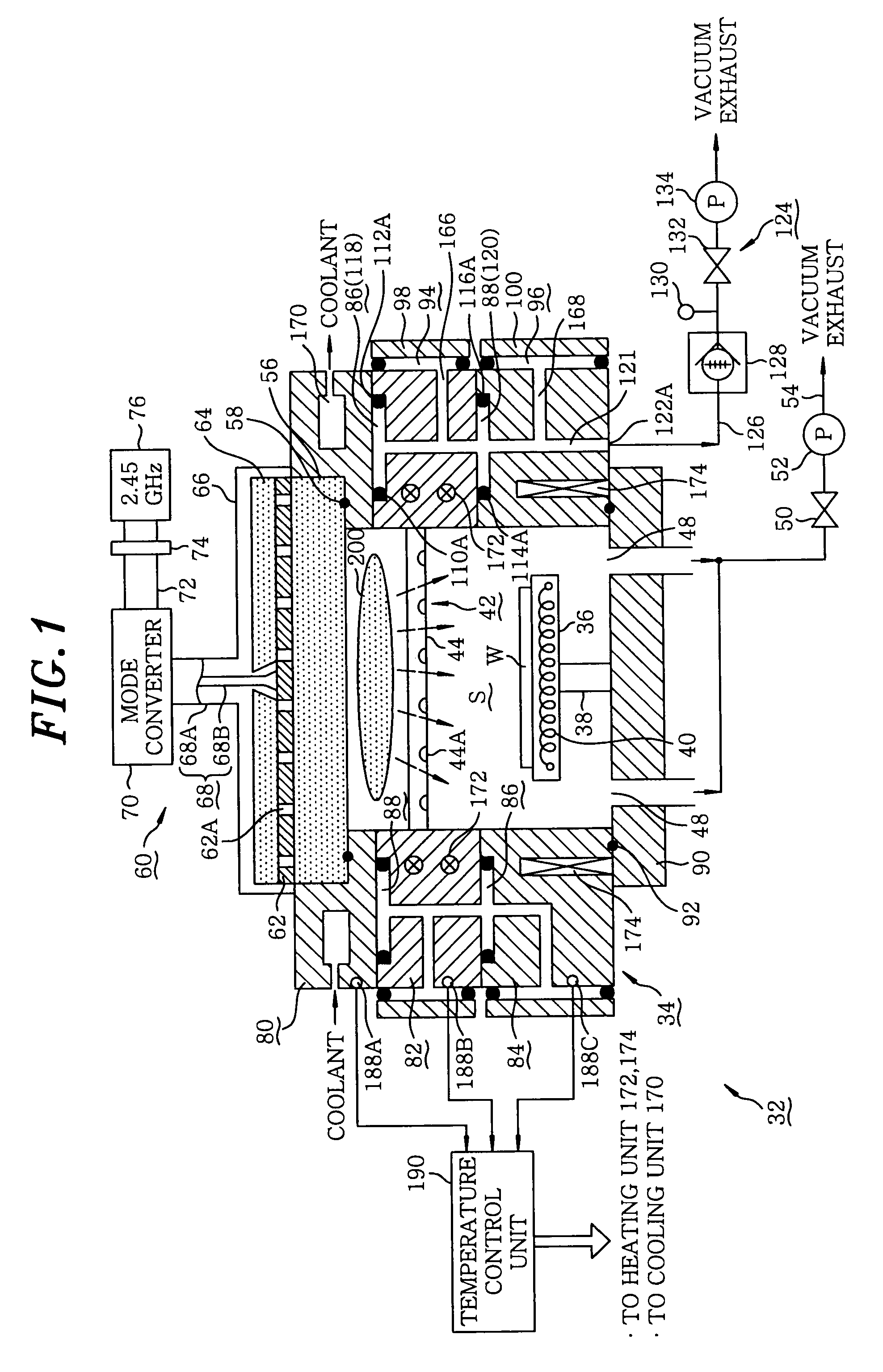
[0009]In view of the problems noted above, it is an object of the present invention to enable temperatures of various portions of a processing vessel to be controlled independently of one another, while improving energy efficiency involved in heating and / or cooling the processing vessel.
[0011]This makes it possible to independently and efficiently control the temperature of the respective block bodies, thanks to the fact that the heat insulating vacuum layer provided between the block bodies suppresses heat transfer between the block bodies.
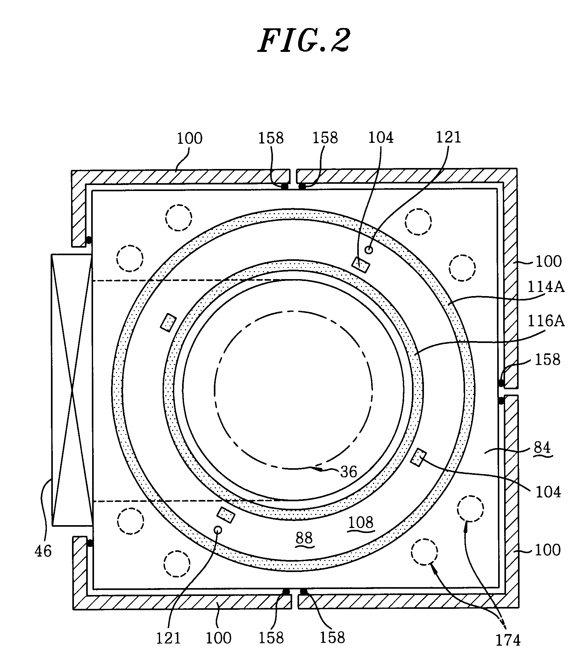
[0016]Preferably, the processing apparatus further including a plasma generating unit for forming electric fields, magnetic fields or electromagnetic fields in the processing vessel to generate plasma within the processing vessel or a plasma introduction unit for supplying plasma generated outside the processing vessel into the processing vessel, and wherein a plasma infiltration prevention ring member for preventing the plasma in the processing vessel from infiltrating into the inter-block gap is provided on an inner side of the seal member lying on the inner peripheral side of the inter-block gap. Preferably, the processing apparatus includes the plasma generating unit, the plasma generating unit including a unit for supplying microwaves or high frequency waves into the processing vessel, and wherein a shield member for electrically connecting the adjoining block bodies to prevent the microwaves or the high frequency waves from leaking to the outside of the processing vessel is provided in the inter-block gap.

Problems solved by technology

For example, if the temperature of the inner sidewall surface of the processing vessel remains low when a fluorocarbon film (interlayer dielectric film) of a low dielectric constant is formed on a wafer by plasma CVD using a CF-based gas, it is highly likely that an unnecessary film is deposited on the inner sidewall surface of the processing vessel.
Furthermore, the unnecessary film adhering thereto at a low temperature is difficult to dislodge by dry cleaning.
However, the solution noted above suffers from the following problems.
First, since the space existing radially outwardly of the wafer W becomes narrow due to the presence of the inner wall 24, a gas stream flowing around the wafer W is changed and so is the radiant heat impinging on the wafer W. This may possibly reduce the in-plane uniformity of a film thickness.
Furthermore, even though the inner wall 24 is heated up, it is unavoidable that an unnecessary film is deposited on the inner wall 24 in the course of processing a large number of wafers.
If the distance between the wafer W and the inner wall 24 is small as noted above, there is also a possibility that the reproducibility of a film thickness becomes worse due to the change in a surface state of the inner wall, which would be caused by deposition of the unnecessary film.
Although the above problems could be solved by increasing the size of the processing vessel 4 in proportion to the installation space of the inner wall 24, this is undesirable in that an increase in the size of the processing vessel 4 leads to an increase in the footprint of a processing apparatus.
Moreover, if a cooling operation of the sidewall of the processing vessel 4 is performed simultaneously with a heating operation of the inner wall 24 arranged adjacent to the processing vessel 4, the heating effect is set off against the cooling effect, thereby posing a problem in that energy efficiency becomes low by the unnecessary consumption of energy.
An additional problem of the structure shown in FIG. 11 is its inability to perform temperature control to intentionally generate a temperature variation in a vertical direction of the processing vessel and, particularly, its inability to locally cool a specified portion.

Method used


Image

  • Processing apparatus
  • Processing apparatus
  • Processing apparatus

Examples


first modified embodiment

[0067]Although the middle block body 82 is formed of a single piece in the foregoing embodiment, it may be possible to fabricate the middle block body 82 from a plurality of, e.g., three, mutually layered pieces 82A, 82B and 82C as illustrated in FIG. 7. In this case, seal members 202 such as O-rings or the like are provided between the adjoining pieces 82A, 82B and 82C to seal off the gaps between the pieces. The adjoining pieces 82A, 82B and 82C are brought into metal-to-metal contact with one another to assure good heat transferability between the pieces. Shield members for preventing leakage of the microwaves may be interposed between the adjoining pieces as is the case in the foregoing embodiment. If the middle block body 82 is constructed by combining the plurality of pieces together, it becomes possible to endow each of the pieces with a special function. As an example, a gas ring structure for supplying a cleaning gas may be provided by forming a plurality of gas injection h...

second modified embodiment

[0068]In the event that the interior of the processing vessel 34 is subjected to, e.g., maintenance and repair in the processing apparatus described above and illustrated in FIGS. 1 to 7, the ceiling plate 56 is separated together with the upper block body 80 provided in the ceiling portion of the processing vessel 34 to thereby open the processing vessel 34 and, then, an operator is allowed to perform a maintenance and repair operation within the processing vessel 34.

[0069]However, since the shower head 44 is fixedly secured to the middle block body 82 in this case, it is quite difficult to conduct the maintenance and repair operation. Further, the maintenance and repair operation becomes highly onerous because the shower head 44 needs to be removed depending on the circumstances. Moreover, a cumbersome operation of adjusting the gaps of the heat insulating gaps present between the upper block body 80 and the middle block body 82 needs to be performed when re-assembling the upper b...


PUM

PropertyMeasurementUnit
thicknessaaaaaaaaaa
temperatureaaaaaaaaaa

Abstract

Provided is a structure of an improved processing vessel for a processing apparatus which processes a target object, such as a semiconductor wafer, which is heated in the metal cylindrical shaped processing vessel by using a processing gas. The processing vessel (34) is composed of a plurality of block bodies (80, 82, 84) mutually connected by being stacked in the vertical direction. Heat insulating vacuum layers (86, 88) are arranged between the adjacent block bodies. Thus, heat transfer between block bodies is suppressed, so that temperature of each block body can be separately controlled, thereby improving energy efficiency.

Description

FIELD OF THE INVENTION[0001]The present invention relates to a processing apparatus for use in performing a specified processing on a target object such as a semiconductor wafer or the like.BACKGROUND OF THE INVENTION[0002]In general, for the manufacture of semiconductor products such as an integrated circuit and the like, various processings including a film forming processing, an oxidation diffusion processing, an etching processing, a quality modification processing and an annealing processing are repeatedly carried out to a semiconductor wafer such as a silicon substrate or the like. A plasma processing apparatus is often used in performing processings of film forming, etching and ashing (see, e.g., JP2003-257933A). In recent years, there is a tendency to frequently use a microwave plasma processing apparatus, owing to an advantage that the apparatus is capable of stably generating high density plasma even in a high vacuum state of about 0.1 mTorr (13.3 mPa) to several tens of m...

Claims


Application Information

Patent Timeline
Patent Type & Authority Applications(United States)
IPC IPC(8): C23F1/08C23C16/00B05C11/00
CPCC23C16/4411C23C16/46H01J37/32522H01J37/32192C23C16/511
Inventor NISHIMOTO, SHINYAYUASA, TAMAKI
Owner TOKYO ELECTRON LTD
Learn More