Charge Domain Filter Circuit

Inactive Publication Date: 2009-05-28
SONY CORP
View PDF5 Cites 10 Cited by
  • Summary
  • Abstract
  • Description
  • Claims
  • Application Information

AI Technical Summary

Benefits of technology

[0018]According to the embodiments of the present invention described above, a charge domain filter circuit can be provided that is new

Problems solved by technology

For example, in a case where the clock signal is operated at a high speed on the order of gigahertz, an increase in the amount of electric current consumed in the logic circuit leads to an increase in the amount of electric power consumed.
Further, if the cycle of the cloc

Method used


Image

  • Charge Domain Filter Circuit
  • Charge Domain Filter Circuit
  • Charge Domain Filter Circuit

Examples


first embodiment

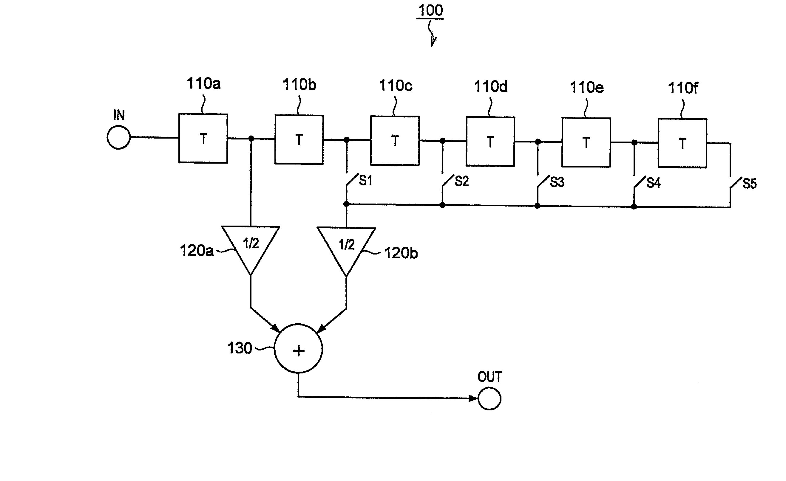
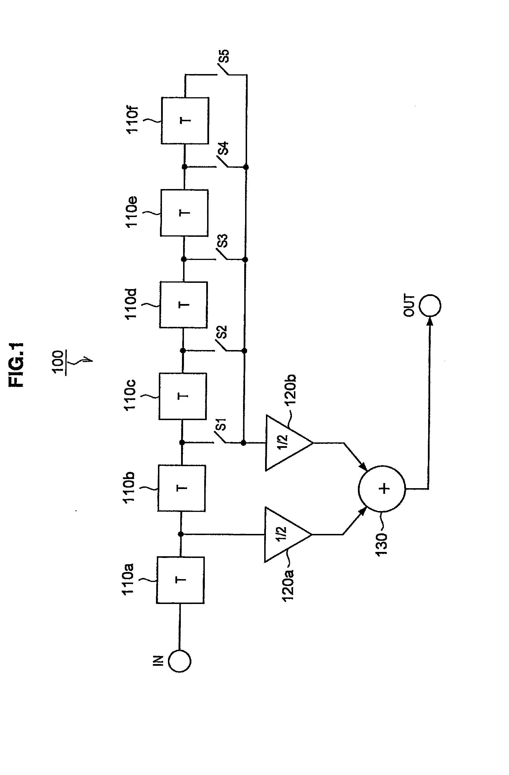
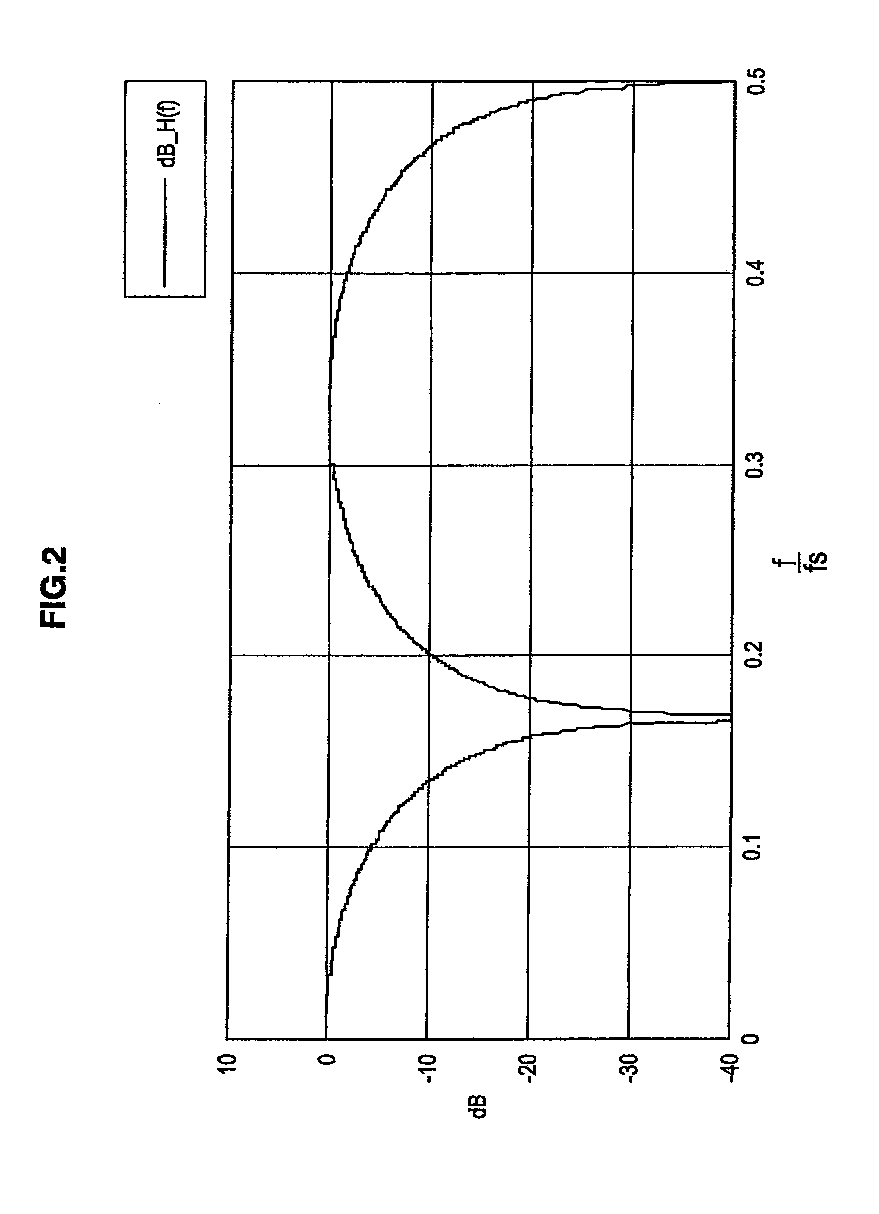
[0045]First, a charge domain filter circuit according to a first embodiment of the present invention will be explained. FIG. 1 is an explanatory figure that uses a block diagram to explain a configuration of a charge domain filter circuit 100 according to the first embodiment of the present invention. The charge domain filter circuit 100 according to the first embodiment of the present invention will be explained below using FIG. 1.

[0046]As shown in FIG. 1, the charge domain filter circuit 100 according to the first embodiment of the present invention is an example of a finite impulse response (FIR) filter and is configured such that it includes delay registers 110a, 110b, 110c, 110d, 110e, 110f, switches S1, S2, S3, S4, S5, multipliers 120a, 120b, and an adder 130.

[0047]A discrete-time signal that is sampled from a continuous-time signal at a sampling interval T is input from an input terminal IN to the charge domain filter circuit 100. The sampling frequency is expressed as fs (1 / ...

second embodiment

[0070]The charge domain filter circuit 100 that was explained in the first embodiment of the present invention can change the frequency characteristics by integrating two signals that are sampled at different times and switching the sampling timing of one of the signals. In a second embodiment of the present invention, a charge domain filter circuit will be explained that can change the frequency characteristics by integrating three signals that are sampled at different times.

[0071]FIG. 7 is an explanatory figure that uses a block diagram to explain a configuration of a charge domain filter circuit 200 according to the second embodiment of the present invention. The charge domain filter circuit 200 according to the second embodiment of the present invention will be explained below using FIG. 7.

[0072]As shown in FIG. 7, the charge domain filter circuit 200 according to the second embodiment of the present invention is an example of a FIR filter and is configured such that it includes...

third embodiment

[0103]The charge domain filter circuit 200 that was explained in the second embodiment of the present invention can change the frequency characteristics by integrating three signals that are sampled at different times. In a third embodiment of the present invention, a charge domain filter circuit will be explained that can change the frequency characteristics by integrating four signals that are sampled at different times.

[0104]FIG. 13 is an explanatory figure that uses a block diagram to explain a configuration of a charge domain filter circuit 300 according to the third embodiment of the present invention. The charge domain filter circuit 300 according to the third embodiment of the present invention will be explained below using FIG. 13.

[0105]As shown in FIG. 13, the charge domain filter circuit 300 according to the third embodiment of the present invention is an example of a FIR filter and is configured such that it includes delay registers 310a, 310b, 310c, 310d, multipliers 32...


PUM


Abstract

A charge domain filter circuit includes a first signal output portion, a second signal output portion, and an adder portion. The first signal output portion outputs a first signal that is sampled at a specified time interval. The second signal output portion outputs a second signal that is sampled at the same time interval as the first signal and at a different time. The adder portion adds the first signal and the second signal together and outputs the result. The second signal output portion is capable of selecting the time to sample the second signal from among a plurality of times.

Description

CROSS REFERENCES TO RELATED APPLICATIONS[0001]The present invention contains subjected matter related to Japanese Patent Application JP 2007-304984 filed in the Japan Patent Office on Nov. 26, 2007, the entire contents of which being incorporated herein by reference.BACKGROUND OF THE INVENTION[0002]1. Field of the Invention[0003]The present invention relates to a charge domain filter circuit.[0004]2. Description of the Related Art[0005]The miniaturization of the complementary metal oxide semiconductor (CMOS) process has the disadvantage that using known circuit technology to implement the RF circuit to reduce the power supply voltage reduces the dynamic range of the signal amplitude, because there is little voltage allowance. On the other hand, because miniaturization raises the cutoff frequency of the transistor, it is suitable for operations such as high-speed switching that must be performed with precise timing. Another advantage is that, because the lithography is performed with...

Claims


Application Information

Patent Timeline
IPC IPC(8): H03K5/01
CPCH03H19/004H03H15/00H03L7/085H03L7/091
Inventor IIDA, SACHIOYOSHIZAWA, ATSUSHI
Owner SONY CORP
Why Eureka
Try Eureka