TFT arrangement for display device

a display device and arrangement technology, applied in static indicating devices, instruments, optics, etc., can solve problems such as display defects, difficult to arrange all tfts apart from the joint portion, etc., to reduce the aperture ratio, increase the distance between regions, and increase the alignment margin

Active Publication Date: 2009-06-04
SEMICON ENERGY LAB CO LTD
View PDF27 Cites 52 Cited by
  • Summary
  • Abstract
  • Description
  • Claims
  • Application Information

AI Technical Summary

Benefits of technology

[0015]That is, in the present invention, a plurality of TFTs, which control the sub-pixels, is arranged collectively so as to surround the intersection portion of the scanning line and the signal line to increase the distance between regions each provided with the plurality of TFTs, whereby the present invention solves the above-described problem. The distance between regions each provided with the plurality of TFTs is large compared with the case where the TFTs are evenly spaced in the display portion, which can prevent the TFT from overlapping with the joint portion between the adjacent SOI

Problems solved by technology

Therefore, when a display device is manufactured using a large SOI substrate which is formed by bonding a plurality of single crystal semiconductor substrates to a large glass substrate, it is difficult to arrange all TFTs

Method used


Image

  • TFT arrangement for display device
  • TFT arrangement for display device
  • TFT arrangement for display device

Examples


embodiment mode 1

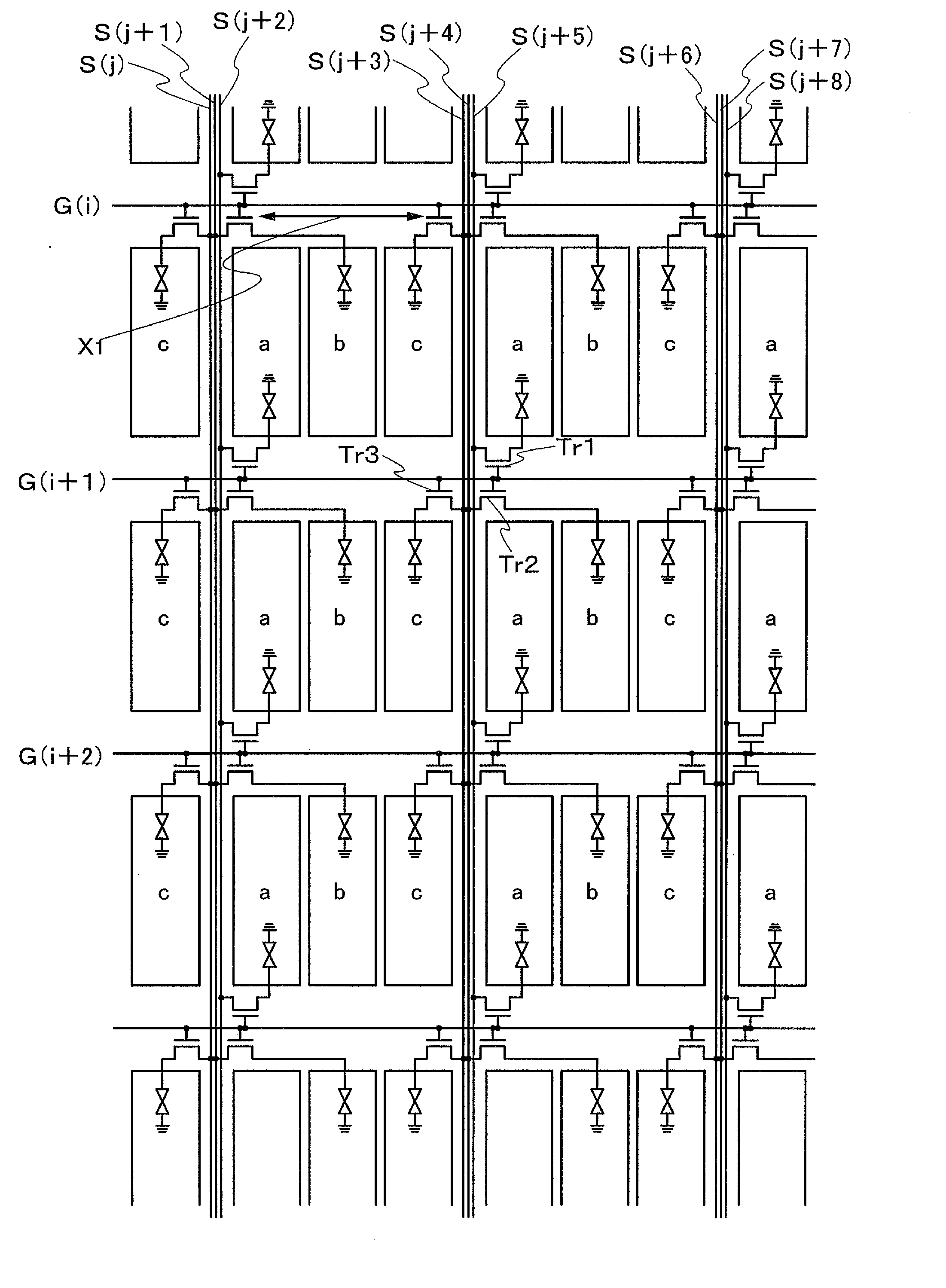
[0034]FIG. 1 is a schematic view illustrating an example of a structure of an active matrix display device according to one mode of the present invention. A pixel of this embodiment mode has a structure in which three sub-pixels each having a rectangular shape or a shape similar to the rectangular shape, that is, “a” (also referred to as a first sub-pixel), “b” (also referred to as a second sub-pixel), and “c” (also referred to as a third sub-pixel) are arranged in a stripe pattern so that the long side of the sub-pixel is parallel to a signal line and in which three signal lines are close to each other and interposed between adjacent pixels.

[0035]Note that a specific structure of the sub-pixels “a”, “b”, and “c” is not limited. For example, R (red), G (green), and B (blue) can be applied to the three sub-pixels.

[0036]A TFT which is provided at the first sub-pixel of a first pixel arranged in a region surrounded by a scanning line G(i), a scanning line G(i+1), signal lines S(j+3) to...

embodiment mode 2

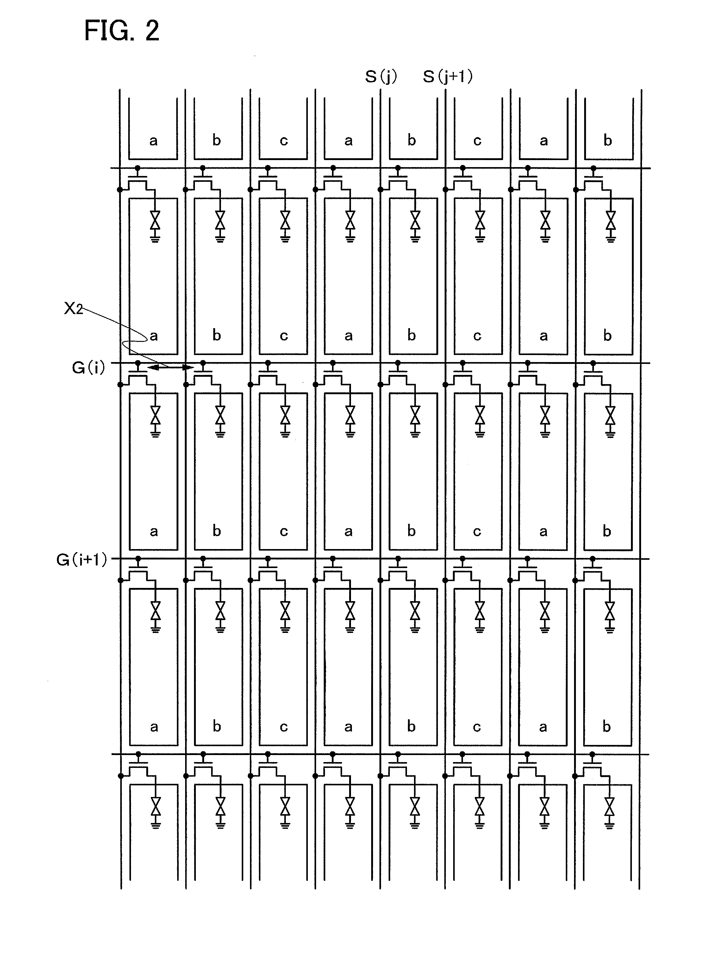
[0042]FIG. 3 is a schematic view illustrating an example of a structure of an active matrix display device according to one mode of the present invention. A pixel of this embodiment mode has a structure in which three sub-pixels having a rectangular shape or a shape similar to the rectangular shape, that is, “a” (also referred to as a first sub-pixel), “b” (also referred to as a second sub-pixel), and “c” (also referred to as a third sub-pixel) are arranged in a stripe pattern so that the long side of the sub-pixel is parallel to a scanning line and in which three scanning lines are close to each other and interposed between adjacent pixels.

[0043]Note that a specific structure of the sub-pixels “a”, “b”, and “c” is not limited. For example, R (red), G (green), and B (blue) can be applied to the three sub-pixels.

[0044]A TFT which is provided at the first sub-pixel of a first pixel arranged in a region surrounded by scanning lines G(i) to G(i+2), scanning lines G(i+3) to G(i+5), a sig...

embodiment mode 3

[0048]FIG. 5 is a view illustrating an example of a structure in which four TFTs are arranged in the periphery of an intersection portion of a scanning line and a signal line in an active matrix display device. A pixel of this embodiment mode has a structure in which three sub-pixels each having a rectangular shape or a shape similar to the rectangular shape, that is, “a” (also referred to as a first sub-pixel), “b” (also referred to as a second sub-pixel), and “c” (also referred to as a third sub-pixel) are arranged in a stripe pattern so that the long side of the sub-pixel is parallel to a signal line and in which four signal lines are close to each other and interposed between adjacent pixels.

[0049]In other words, the pixel of this embodiment mode has a structure in which four sub-pixels having a rectangular shape or a shape similar to the rectangular shape, that is, “a” (also referred to as a first sub-pixel), “b” (also referred to as a second sub-pixel),“c” (also referred to as...


PUM


Abstract

A new TFT arrangement is demonstrated, which enables prevention of TFT to be formed over a joint portion between the adjacent SOI layers prepared by the process including the separation of a thin single crystal semiconductor layer from a semiconductor wafer. The TFT arrangement is characterized by the structure where a plurality of TFTs each belonging to different pixels is gathered and arranged close to an intersection portion of a scanning line and a signal line. This structure allows the distance between regions, which are provided with the plurality of TFTs, to be extremely large compared with the distance between adjacent TFTs in the conventional TFT arrangement in which all TFTs are arranged in at a regular interval. The formation of a TFT over the joint portion can be avoided by the present arrangement, which leads to the formation of a display device with a negligible amount of display defects.

Description

TECHNICAL FIELD[0001]The present invention relates to a display device having a so-called SOI (silicon on insulator) structure in which a semiconductor layer is provided over an insulating surface.BACKGROUND ART[0002]An integrated circuit has been developed, which uses a semiconductor substrate so-called a silicon-on-insulator (hereinafter also referred to as an SOI) that has a thin single crystal semiconductor layer over an insulating surface, as an alternative to a silicon wafer that is manufactured by thinly slicing an ingot of a single crystal semiconductor. The integrated circuit using the SOI substrate attracts much attention because the use of the SOI substrate enables the reduction of parasitic capacitance between a drain of a transistor and the substrate, which contributes to the improvement in performance of a semiconductor integrated circuit.[0003]There are various methods for manufacturing an SOI substrate, and Smart Cut (registered trademark) is known as a method which ...

Claims


Application Information

Patent Timeline
IPC IPC(8): H01L29/04H05B44/00
CPCH01L27/1214H01L27/1266H01L29/78654H01L51/5284H01L27/3276H01L27/3218H01L27/326H01L27/3262H01L27/3213H01L27/124H10K59/351H10K59/353H10K59/121H10K59/1213H10K59/131H10K50/865G02F1/134336G02F2201/52G02F1/134309G09G3/3614G09G3/3659G09G3/3611G09G3/3607G02F1/134345G02F1/136286G02F1/1368
Inventor KASAHARA, TAKAHIRO
Owner SEMICON ENERGY LAB CO LTD
Why Eureka
Try Eureka