Film formation method, thin-film transistor and solar battery

a technology of thin-film transistors and solar cells, applied in the manufacture of final products, basic electric elements, coatings, etc., can solve the problems of unstable operation characteristics of thin-film transistors, physical and electrical bonding between crystal grains weakened, and difficulty in manufacturing transistors, so as to improve the operation characteristics of tft and ensure stability

Inactive Publication Date: 2009-06-04
TOKYO ELECTRON LTD
View PDF1 Cites 5 Cited by
  • Summary
  • Abstract
  • Description
  • Claims
  • Application Information

AI Technical Summary

Benefits of technology

[0004]However, since crystal grains of the microcrystalline film grow in a columnar manner, physical and electrical bonding between the crystal grains is weakened. For this reason, as shown about the microcrystalline film (single-layer film) and mobility in an upper portion of FIG. 14, a barrier h is present at a grain boundary between adjacent ones of the crystal grains. For this reason, when a carrier composed of an electron and hole moves across the grain boundary of the microcrystalline film, electrical resistance in a horizontal direction of the film increases. Whenever the carrier traverses the barrier h, a mobility μ is reduced. An operation of the thin-film transistor is thereby delayed. As a result of this delay, operation characteristics of the thin-film transistor are rendered unstable.
[0006]In view of the issue described above, the present invention provides a method of forming a microcrystalline silicon film of which electrical and physical characteristics are rendered satisfactory by improving a horizontal bonding strength between crystal grains that form the microcrystalline film.
[0012]With this arrangement, electrical and physical bonding between crystal grains in the horizontal direction is strengthened by the stacked-layer film of the microcrystalline film and the ultra-microcrystalline film. The operation characteristics of the TFT may be thereby improved. Further, the substrate, which is the base of the microcrystalline silicon film may be prevented from being etched by the chemical solution. The TFT may be thereby stably manufactured.

Problems solved by technology

However, since crystal grains of the microcrystalline film grow in a columnar manner, physical and electrical bonding between the crystal grains is weakened.
As a result of this delay, operation characteristics of the thin-film transistor are rendered unstable.
The transistor may be thereby difficult to manufacture.
Thus, electrical and physical characteristics of the thin-film transistor deteriorate at the grain boundaries.

Method used


Image

  • Film formation method, thin-film transistor and solar battery
  • Film formation method, thin-film transistor and solar battery
  • Film formation method, thin-film transistor and solar battery

Examples


first embodiment

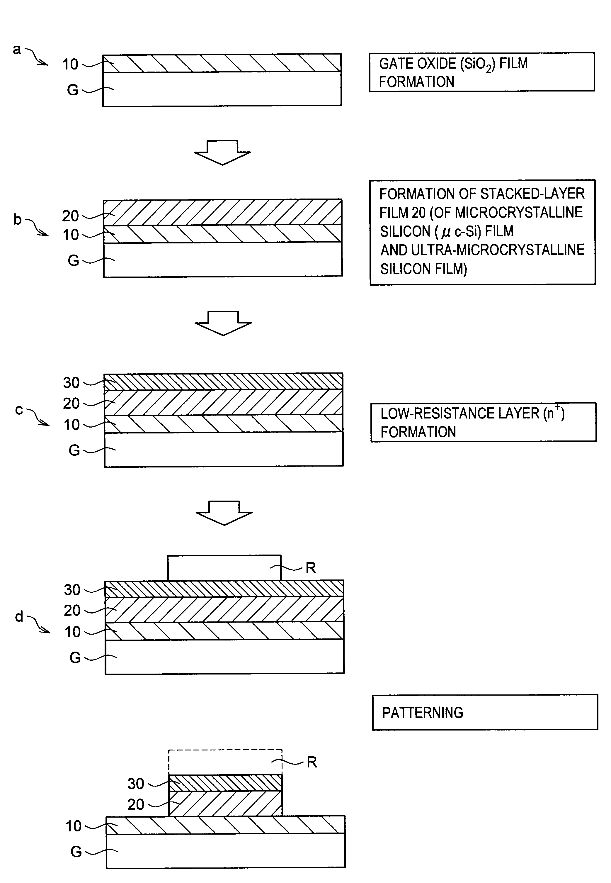
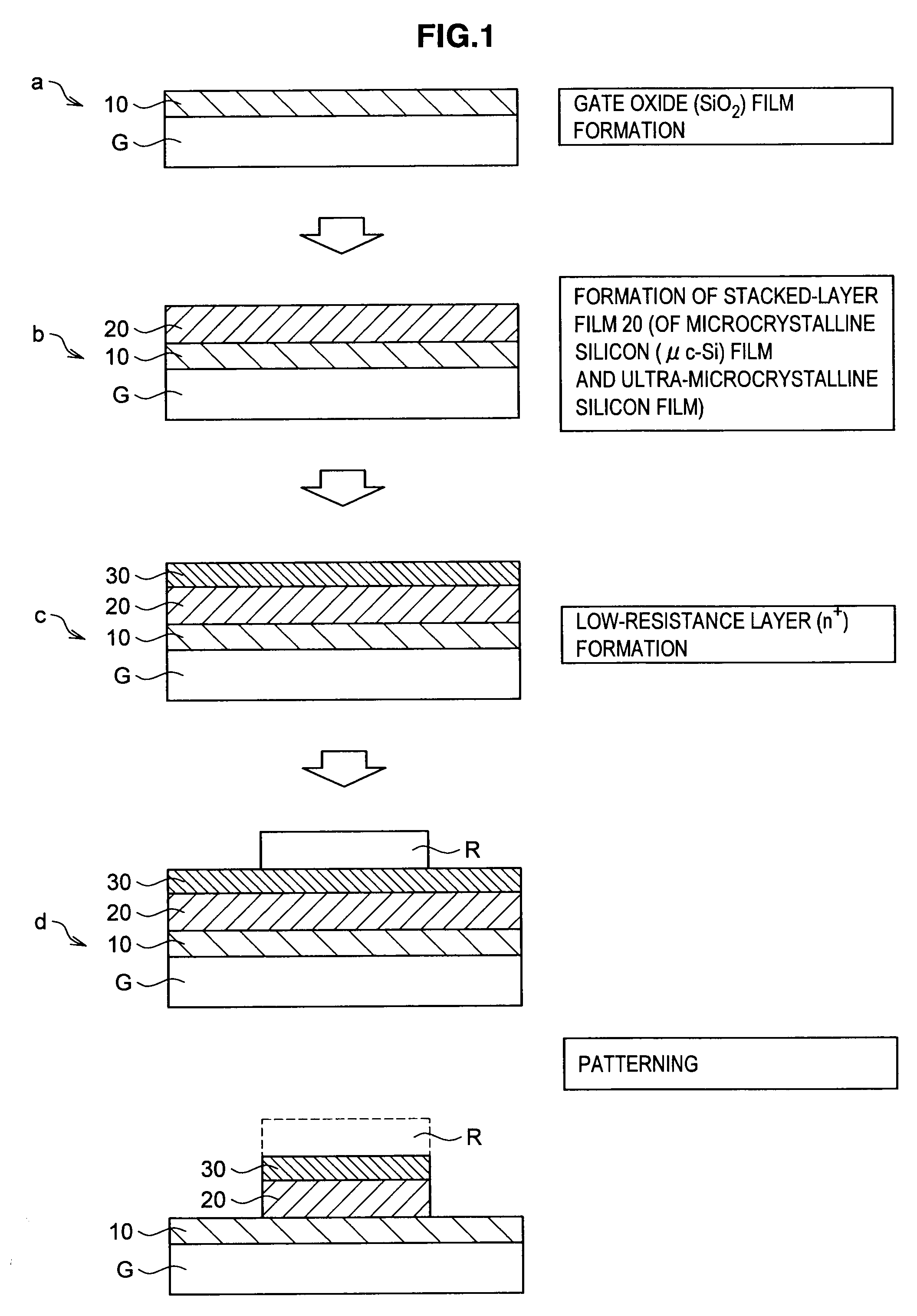
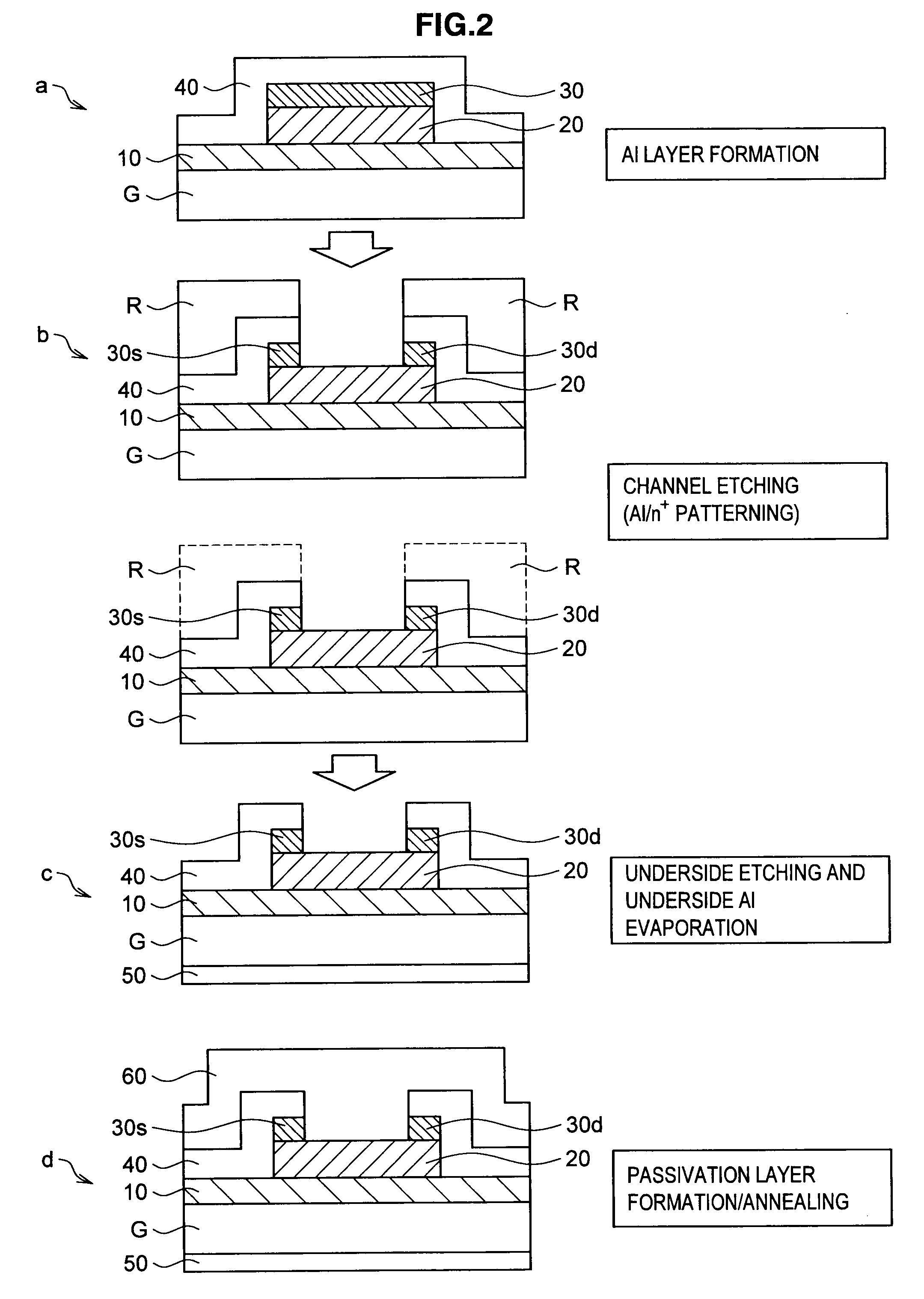
[0028]In a TFT manufacturing process in this embodiment, a bottom-gate type TFT (doped silicon substrate) where a gate electrode is disposed below a microcrystalline silicon film is manufactured. The microcrystalline silicon film is formed as an active layer. In FIGS. 1 and 2, a bottom-gate type TFT manufacturing process is illustrated. In FIGS. 1 and 2, respective steps of the process of manufacturing the TFT of an n-channel type are shown. When an impurity to be doped is changed, the TFT of a p-channel type may be manufactured, using the respective steps in FIGS. 1 and 2.

1. Gate Oxide Film Formation

[0029]In the bottom-gate type TFT manufacturing process, a gate oxide (SiO2) film 10 is first formed on a silicon substrate G, in step a in FIG. 1. The gate oxide film 10 is deposited on the silicon substrate G into which phosphor (P) has been doped. The doped silicon film is a low-resistance layer (n+). The gate oxide film 10 is deposited to a thickness of 100 nm with plasma under low ...

second embodiment

[0105]In the first embodiment, depositing the stacked-layer film of the microcrystalline silicon film and the ultra-microcrystalline silicon film as the active layer, the TFT with the high mobility μ and the high on / off current ratio and strong BHF resistance could be manufactured. Based on this result, the inventor has considered whether there is an optimal film thickness combination between the microcrystalline silicon film and the ultra-microcrystalline silicon film. Then, in a second embodiment, an experiment and a result of the experiment conducted by the inventor in order to obtain a proper film thickness combination between the microcrystalline silicon film and the ultra-microcrystalline silicon film will be described.

[0106]The inventor changed a deposition time of each film in order to change a film thickness combination between the two types of films. Specifically, the deposition time of the microcrystalline film (first film) was changed to 5 seconds, 10 seconds, and 15 sec...


PUM

PropertyMeasurementUnit
electron densityaaaaaaaaaa
temperatureaaaaaaaaaa
thicknessaaaaaaaaaa

Abstract

After a gate oxide film 10 has been formed on a silicon substrate G, a first step of forming a microcrystalline silicon film by high electron density plasma of an electron temperature of 2.0 eV or less and a second step of forming an ultra-microcrystalline silicon film by high electron density plasma of an electron temperature higher than 2.0 eV are repeated. A stacked-layer film 20 of the ultra-microcrystalline silicon film and the microcrystalline silicon film is thereby formed. With the film formation method described above, at least one of an n-channel thin-film transistor and a p-channel thin-film transistor with the stacked-layer film 20 functioned as an active layer may be manufactured.

Description

CROSS-REFERENCE TO RELATED APPLICATION[0001]The present invention contains subject matter related to Japanese Patent Application JP 2007-310264, filed in the Japan Patent Office on Nov. 30, 2007, the entire contents of which being incorporated herein by reference.FIELD OF THE INVENTION[0002]The present invention relates to a film formation method. More specifically, the invention relates to a method of forming a film used for a thin-film transistor or a solar battery.BACKGROUND OF THE INVENTION[0003]Among silicon oxide films used for an active layer of the thin-film transistor are an amorphous silicon film (a-Si), a poly-silicon (Poly-Si) film, and a microcrystalline silicon film (μc-Si). The amorphous silicon film is an amorphous film, the poly-silicon film is a poly-crystal film, and the microcrystalline silicon film is a microcrystalline film. Among these films, the microcrystalline film has a higher mobility than the amorphous film. The microcrystalline film does not necessarily...

Claims


Application Information

Patent Timeline
Patent Type & Authority Applications(United States)
IPC IPC(8): H01L21/20H01L29/04H01L31/0368
CPCH01L21/02532H01L21/02595H01L21/0262H01L29/04Y02E10/548H01L29/78696H01L31/03685H01L31/1824Y02E10/545H01L29/66765Y02P70/50H01L21/2053
Inventor OKA, SHINSUKE
Owner TOKYO ELECTRON LTD
Why Eureka
Try Eureka