Method of Film Deposition and Film Deposition System

a film deposition and film technology, applied in the direction of coatings, chemical vapor deposition coatings, metallic material coating processes, etc., can solve the problems of low step coverage of thin film deposited, extremely low film deposition rate, poor throughput, etc., and achieve high step coverage and film deposition rate

Inactive Publication Date: 2009-06-04
TOKYO ELECTRON LTD
View PDF5 Cites 13 Cited by
  • Summary
  • Abstract
  • Description
  • Claims
  • Application Information

AI Technical Summary

Benefits of technology

[0013]In view of the aforementioned problems in the prior art and in order to solve them effectively, we accomplished the present invention. Accordingly, an object of the present invention is to provide a method of film deposition and a film decomposition system that can ensure high step coverage and high film deposition rate.
[0015]According to the present invention, the step coverage can be kept high by alternately carrying out the first and second gas-supplying steps, and the film deposition rate can also be kept high by keeping the temperature of the object to be processed equal to or higher than the decomposition-starting temperature of the high-melting-point organometallic material. Namely, the present invention can have the advantages of both the CVD and ALD methods.

Problems solved by technology

However, since they have become very strict recently and mask patterns prescribed by them have become smaller in line width and higher in aspect ratio, the CVD method has become disadvantageous in that, although a thin film is deposited on the trenched upper surface of a wafer at a relatively high rate, the step coverage of the thin film deposited is low.
The ALD method is thus disadvantageous in that the film deposition rate is extremely low and that the throughput is poor.

Method used


Image

  • Method of Film Deposition and Film Deposition System
  • Method of Film Deposition and Film Deposition System
  • Method of Film Deposition and Film Deposition System

Examples


first embodiment

[0069]The first embodiment of the method of film deposition according to the present invention will be described.

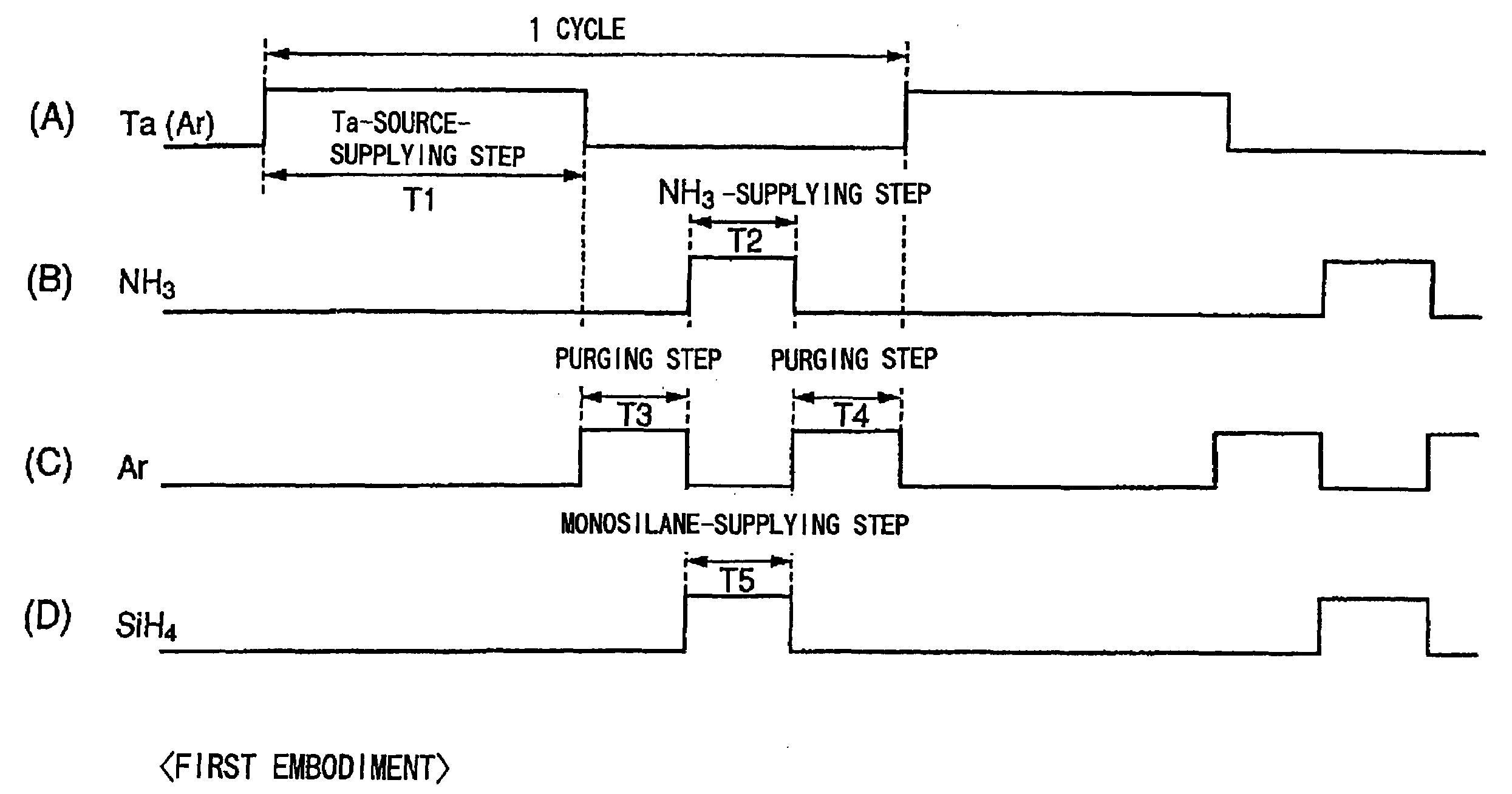
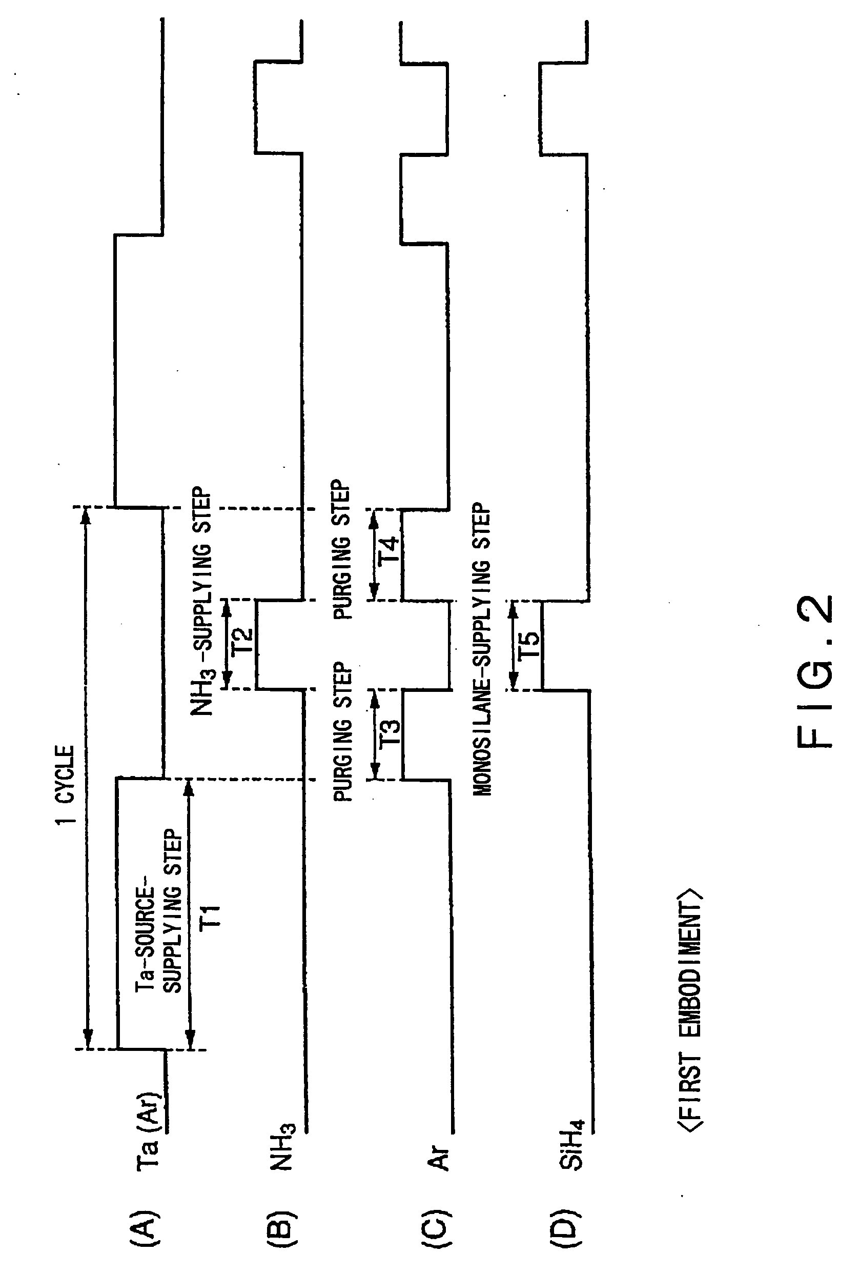
[0070]FIG. 2 is a diagram showing a gas supply mode in the first embodiment of the method of the invention. In the following description, explanation will be given by referring to the case where silicon-containing tantalum nitride film (TaSiN) is formed as a metallic nitride film, a metallic compound film.

[0071]As shown in FIG. 2, a step of supplying the Ta source (FIG. 2(A)) and a step of supplying NH3 gas (FIG. 2(B)) are alternately carried out two or more times. In this embodiment, a purging step of purging the gas remaining in the processing vessel 4 is carried out between the Ta source-supplying step and the NH3 gas-supplying step. In this purging step, Ar gas is fed as a purge gas, as shown in FIG. 2(C), to accelerate exhaust of the gas remaining in the vessel. In this step, it is preferable to purge the vessel to such an extent that the Ta source gas remains in the...

second embodiment

[0109]Next, the second embodiment of the present invention will be described.

[0110]In the first embodiment, the monosilane-supplying step (period T5: FIG. 2(D)) and the NH3-supplying step (period T2: FIG. 2(B)) are simultaneously carried out for the same length of time. However, the present invention is not limited to this. Period T5 may be varied in order to regulate the silicon content of tantalum nitride film containing silicon (TaSiN).

[0111]In this embodiment, the process pressure is preferably in the range of 0.1 to 5 Torr. The wafer temperature is preferably more than 250° C. and 750° C. or less, more preferably more than 250° C. and 550° C. or less. The SiH4 partial pressure in the step of supplying NH3 gas and SiH4 gas is preferably 0.2 Torr or less, or 70% or less of the total pressure, more preferably 0.15 Torr or less, or 50% or less of the total pressure. The NH3 partial pressure is preferably 0.075 Torr or more, or 20% or more of the total pressure. Further, the purge f...

third embodiment

[0115]The third embodiment of the present invention will be described below.

[0116]The first embodiment has been described by referring to the case where silicon-containing tantalum nitride film (TaSiN) is formed as a metallic nitride film, a metallic compound film. The present invention is not limited to this, and silicon-carbon-containing tantalum nitride film (TaSiCN) may also be formed as a metallic nitride film.

[0117]In this embodiment, the process pressure is preferably in the range of 0.1 to 5 Torr. The wafer temperature is preferably more than 250° C. and 750° C. or less, more preferably more than 250° C. and 550° C. or less. The SiH4 partial pressure in the step of supplying NH3 gas and SiH4 gas is preferably 0.2 Torr or less, or 70% or less of the total pressure, more preferably 0.15 Torr or less, or 50% or less of the total pressure. The NH3 partial pressure is preferably 0.075 Torr or more, or 20% or more of the total pressure. The purge flow rate of Ar gas in the purging...


PUM

PropertyMeasurementUnit
diameteraaaaaaaaaa
temperatureaaaaaaaaaa
pressureaaaaaaaaaa

Abstract

The present invention is a method of film deposition that comprises a first gas-supplying step of supplying a high-melting-point organometallic material gas to a processing vessel that can be evacuated, and a second gas-supplying step of supplying, to the processing vessel, a gas consisting of one, or two or more gases selected from a nitrogen-containing gas, a silicon-containing gas, and a carbon-containing gas, wherein a thin metallic compound film composed of one, or two or more compounds selected from a high-melting-point metallic nitride, a high-melting-point metallic silicate, and a high-melting-point metallic carbide is deposited on the surface of an object to be processed, placed in the processing vessel. The first and second gas-supplying steps are alternately carried out, and in these steps, the object to be processed is held at a temperature equal to or higher than the decomposition-starting temperature of the high-melting-point organometallic material.

Description

BACKGROUND OF THE INVENTION[0001]1. Field of the Invention[0002]The present invention relates to a method of film deposition for forming a thin film on an object to be processed, such as a semiconductor wafer, and to a film deposition system.[0003]2. Background Art[0004]Generally, in the production of semiconductor integrated circuits, objects to be processed, such as semiconductor wafers, are repeatedly subjected, sheet by sheet, to various processing steps, such as film deposition, etching, heat treatment, modification, and recrystallization, thereby obtaining desired integrated circuits. Moreover, the recent demand for thinner integrated circuits having higher levels of integration has made the line width, film thickness, etc. of integrated circuits much smaller than ever.[0005]Nitrided films of high-melting-point organometallic materials tend to be often used as materials that show relatively low resistivity even when they are made thinner than ever and patterned to have extreme...

Claims


Application Information

Patent Timeline
Patent Type & Authority Applications(United States)
IPC IPC(8): C23C16/44
CPCC23C16/34C23C16/45531H01L21/76843H01L21/28562C23C16/46H01L21/205
Inventor NAKAMURA, KAZUHITOYAMASAKI, HIDEAKIKAWANO, YUMIKO
Owner TOKYO ELECTRON LTD
Why Eureka
Try Eureka