Method of eliminating a lithography operation

a lithography operation and lithography technology, applied in the field of semiconductor device fabrication techniques, can solve the problems of increasing the resolution limit of conventional optical lithography technology, the inability to project an accurate image of increasingly smaller features onto the wafer, and the skyrocketing overall polygonal figure coun

Active Publication Date: 2009-06-11
CADENCE DESIGN SYST INC
View PDF14 Cites 455 Cited by
  • Summary
  • Abstract
  • Description
  • Claims
  • Application Information

AI Technical Summary

Problems solved by technology

The ability to project an accurate image of increasingly smaller features onto the wafer is limited by the wavelength of the light used, and the ability of the lens system to capture enough diffraction orders from the illuminated mask.
Accordingly, the resolution limit of conventional optical lithography technology is increasingly being challenged by the sub wavelength, or low-k1, dimensions of the critical IC feature geometries.
Furthermore, due to the necessity to mitigate optical proximity effect distortions through resolution enhancement techniques at the mask level, the overall polygonal figure count is skyrocketing.
Extreme precision is required for sub wavelength, or low-k1, applications due to highly non-linear imaging behaviors, which often magnify mask errors by large factors and in non-intuitive manners.
However, such trends have proven difficult for a number of reasons and designers have moved to non-lithographic enhancements to increase pattern density.
As these examples also illustrate, conventional techniques using self-aligned double patterning processes are useful for making lines but have not been used to make arbitrary patterns.

Method used


Image

  • Method of eliminating a lithography operation
  • Method of eliminating a lithography operation
  • Method of eliminating a lithography operation

Examples


Embodiment Construction

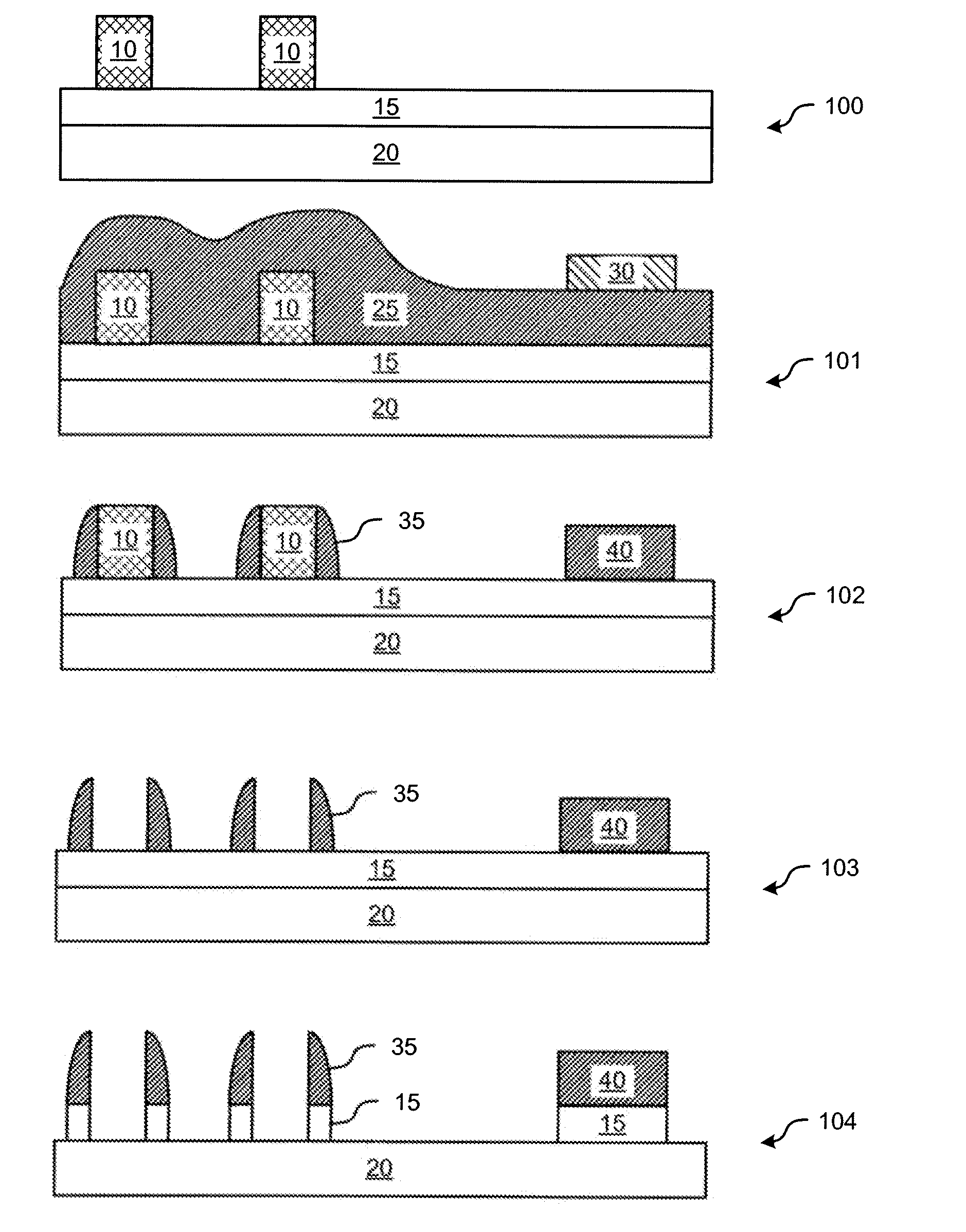
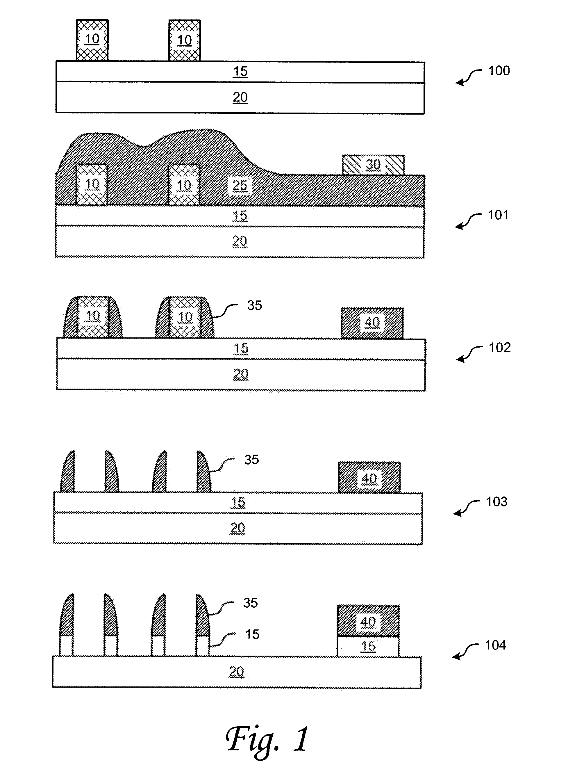
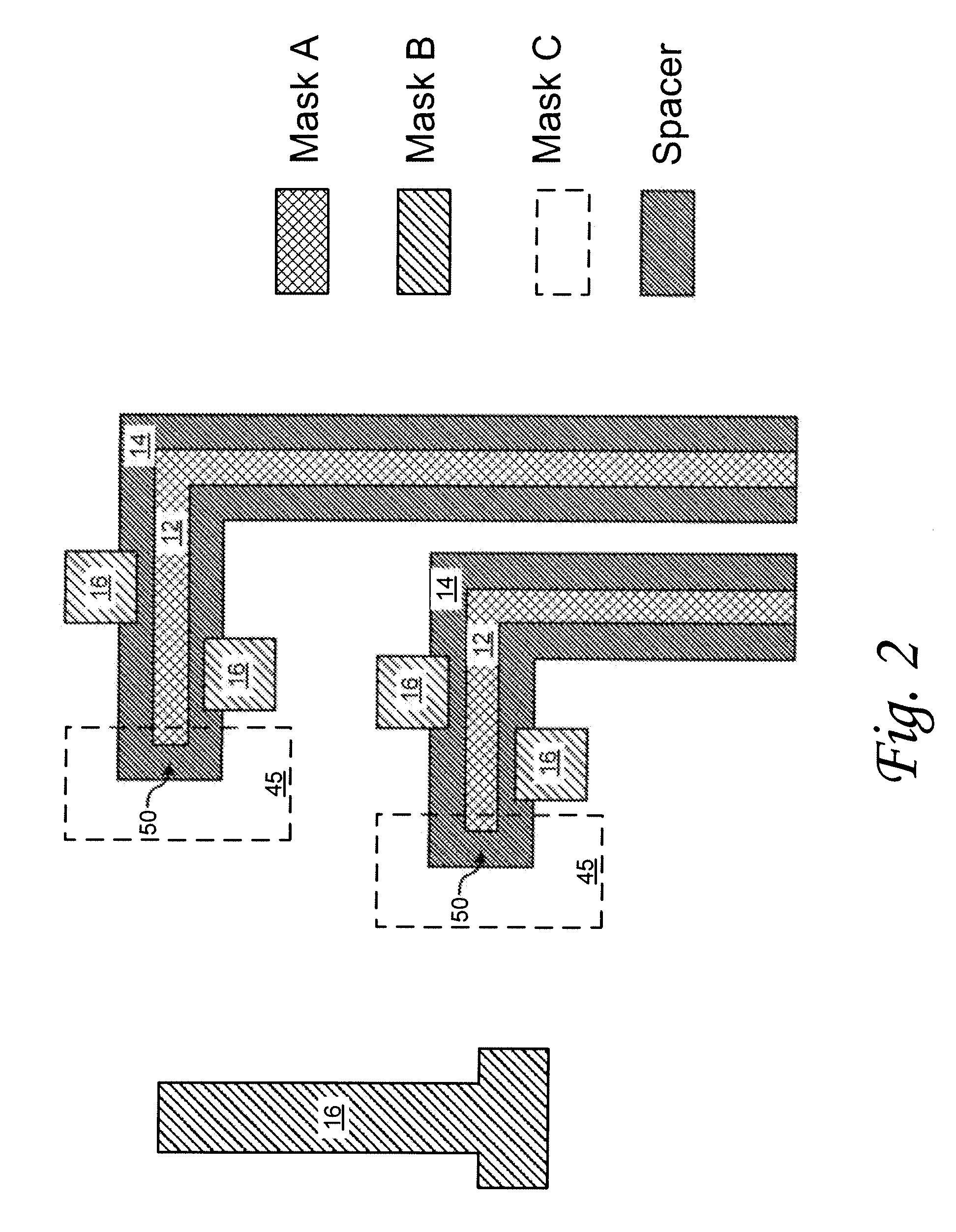
[0014]According to various embodiments of the invention semiconductor devices and methods of manufacture are provided. In one embodiment, lines and components are provided on a layer of a semiconductor device, wherein the lines are of a first width and components, such as contact pads or other components, are of a second width. In accordance with one embodiment of the invention, the lines and contact pads are formed on a layer of the device without the need for an additional mask layer to form the contact pads. In another embodiment, other features in addition to or instead of contact pads can be added in the same mask layer.

[0015]According to an embodiment of the invention a method of semiconductor device fabrication includes processes of depositing a layer of a first material on a semiconductor substrate and patterning the layer to form a first pattern, wherein the first pattern defines wide and narrow space features; depositing spacer material over the first pattern on the substr...


PUM


Abstract

Methods of semiconductor device fabrication are disclosed. An exemplary method includes processes of depositing a first pattern on a semiconductor substrate, wherein the first pattern defines wide and narrow spaces; depositing spacer material over the first pattern on the substrate; etching the spacer material such that the spacer material is removed from horizontal surfaces of the substrate and the first pattern but remains adjacent to vertical surfaces of a wide space defined by the first pattern and remains within narrow a space defined by the first pattern; and removing the first pattern from the substrate. In one embodiment, the first pattern can comprise sacrificial material, which can include, for example, polysilicon material. The deposition can comprise physical vapor deposition, chemical vapor deposition, electrochemical deposition, molecular beam epitaxy, atomic layer deposition or other deposition techniques. According to another embodiment, features for lines and logic device components having a width greater than that of the lines are formed in the spacer material in the same mask layer.

Description

TECHNICAL FIELD [0001]The present invention relates to device manufacturing, and more particularly, some embodiments relate to semiconductor device fabrication techniques.DESCRIPTION OF THE RELATED ART [0002]Integrated circuits, or ICs, are generally created by patterning a plurality of devices and their interconnects onto a substrate such as a semiconductor wafer. This process generally starts with a design for the circuit or circuits that will make up the IC. A top-down design methodology is commonly employed using hardware description languages (HDLs), such as Verilog®, RTM® or VHSIC hardware description language (VHDL), for example. Through the use of HDLs, the designer creates an integrated circuit by hierarchically defining functional components of the circuit.[0003]From the HDL or other high-level description, the actual logic cell implementation may be determined by logic synthesis, which converts the functional description of the circuit into a specific circuit implementati...

Claims


Application Information

Patent Timeline
Patent Type & Authority Applications(United States)
IPC IPC(8): H01L23/48H01L21/311G06F17/50
CPCH01L21/0337H01L21/32139H01L21/0338
Inventor WELING, MILINDSEZGINER, ABDURRAHMAN
Owner CADENCE DESIGN SYST INC
Why Eureka
Try Eureka