Optical multilayer thin-film filters and methods for manufacturing same

a thin-film filter and optical multi-layer technology, applied in the field of multi-layer film optical filters, can solve the problems of adding unwanted color to the detected image, difficult to remove the dust from the filter, and contaminating the interior of the deposited multi-layer film layer, etc., to achieve the effect of eliminating static and high conductivity

Inactive Publication Date: 2009-06-18
NIHON DEMPA KOGYO CO LTD
View PDF4 Cites 14 Cited by
  • Summary
  • Abstract
  • Description
  • Claims
  • Application Information

AI Technical Summary

Benefits of technology

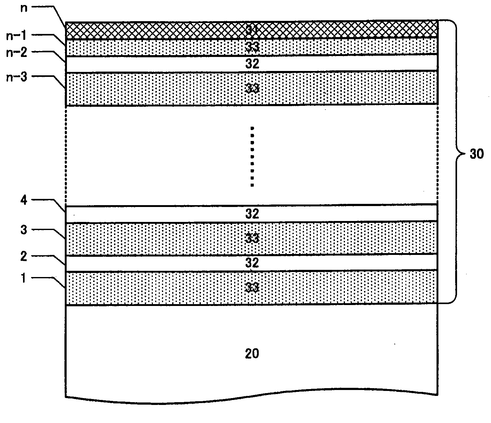
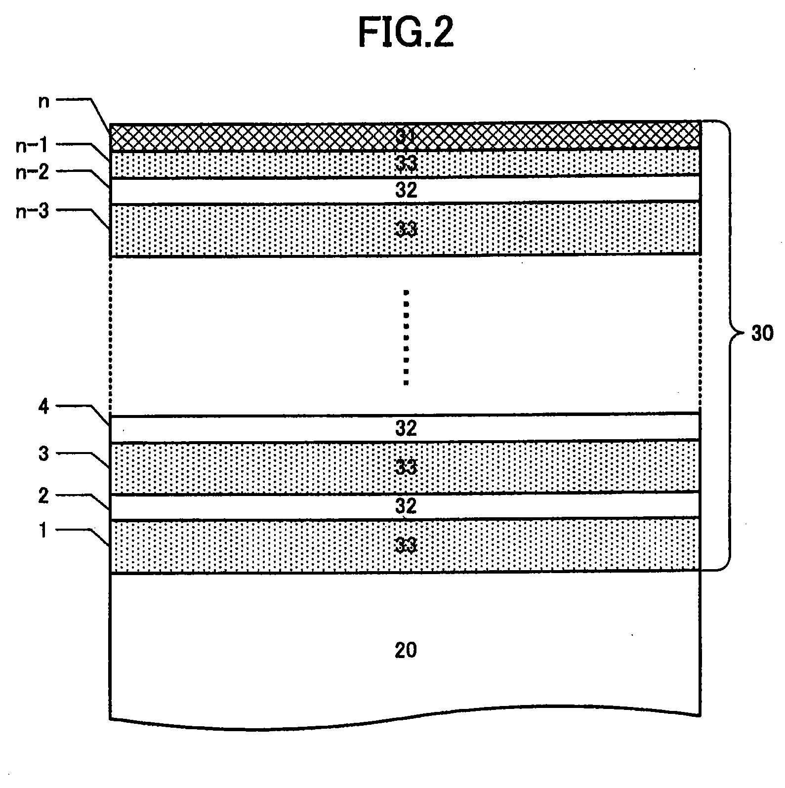
[0014]According to another aspect of the invention, methods are provided for manufacturing an OMTFF. An embodiment of the method includes a first deposition step, in which alternating thin layers of a high-refractive-index material and of a low-refractive-index material are deposited superposedly on a transparent substrate. Thus, in the first deposition step, a multilayer film is formed. In a second deposition step a “top” layer is formed, atop the multilayer film, of a material having a lower molecular weight than either the high- or low-refractive-index materials. In a suppression step the amount of lower-molecular-weight material allowed to diffuse into the high- and low-refractive-index materials is controlled. By appropriate control being exercised in the suppression step, the deposited low-molecular-weight material is substantially prevented from entering the high- and low-refractive-index materials easily, allowing a practical OMTFF to be manufactured.
[0015]The suppression step can include, for example, establishing conditions in which the high- and low-refractive-index materials can absorb moisture. Moisture absorption by the high- and low-refractive-index materials largely prevents the low-molecular-weight material of the top layer from entering the high- and low-refractive-index materials.
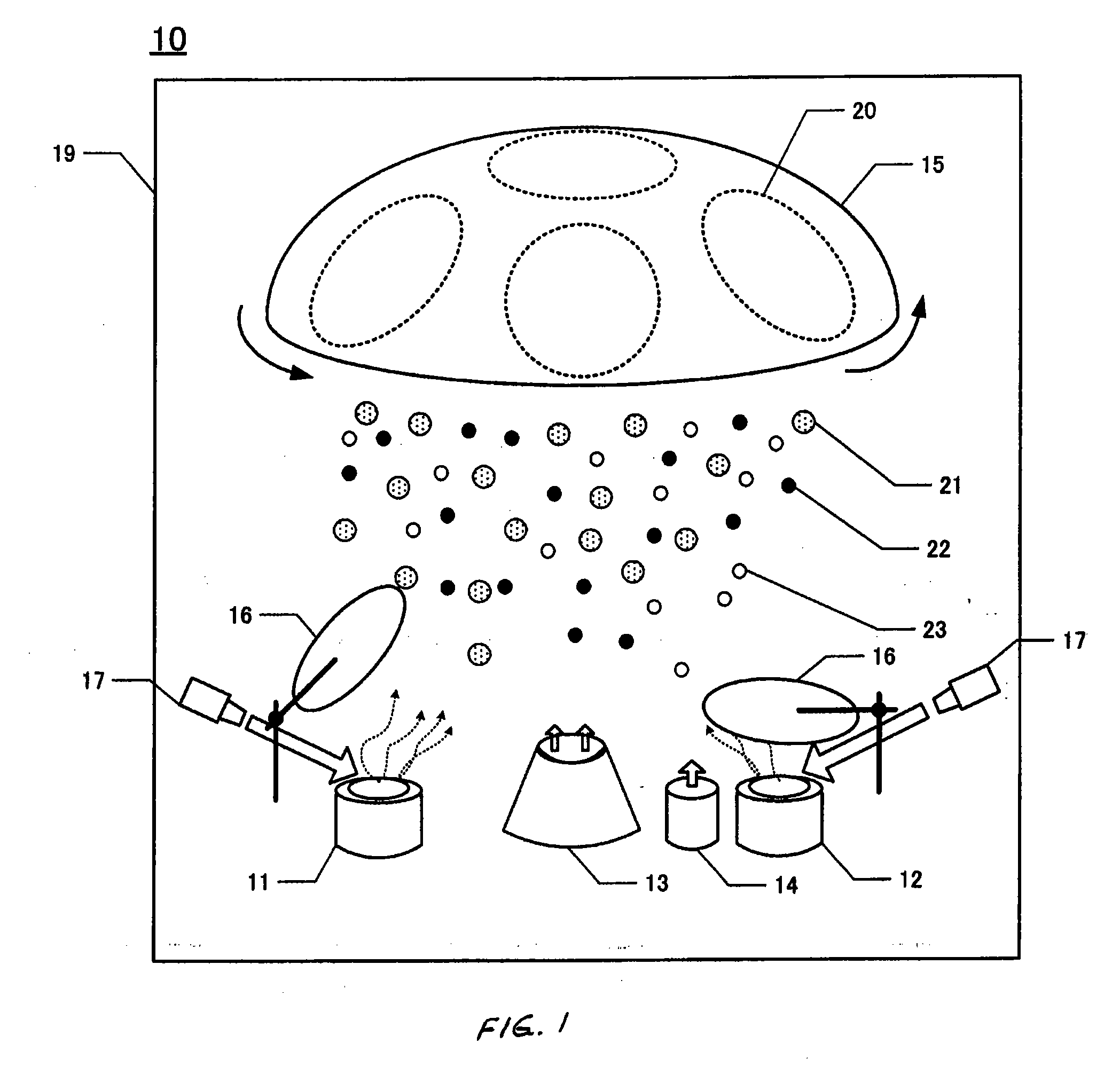
[0016]Desirably, in the first deposition step, the high-refractive-index layers and low-refractive-index layers of the multilayer film are formed alternatingly by vacuum deposition in a vacuum chamber. Then, in a suppression step after the first deposition step, the vacuum chamber is vented to atmosphere. In the subsequent second deposition step, the vacuum chamber is returned to a vacuum state before commencing deposition of the low-molecular-weight material to form the top layer. By venting the chamber to atmosphere during the suppression step, moisture contained in the air is absorbed in the layers of high- and low-refractive-index materials. With this simple venting step an OMTFF is fabricated that has high conductivity.
[0017]Various embodiments of an OMTFF include a metal film formed without having to use a transparent electrode material such as ITO in the top (also called “final”) layer. Thus, the surface of the OMTFF effectively eliminates static from the OLPF with which the OMTFF is often used.

Problems solved by technology

The sensor also tends to generate color moire patterns that add unwanted color to the detected image when the photographic subject has large luminance differences such as hair illuminated by backlight.
The adsorbed dust also tends to be charged, making it difficult to remove the dust from the filter.
However, strictly speaking, the method of depositing ITO tends to contaminate the interior of the deposited multilayer-film layers.
The contamination tends to degrade the optical performance of the OMTFF.
Contamination arises because ITO is deposited on the surface of the multilayer film after forming the multilayer film.
Also, indium (In) is a rare metal; since ITO is used for liquid-crystal panels and flat-panel displays (FPDs) such as organic EL, its anticipated price escalation and deficiency of supply in the future is a concern.

Method used


Image

  • Optical multilayer thin-film filters and methods for manufacturing same
  • Optical multilayer thin-film filters and methods for manufacturing same
  • Optical multilayer thin-film filters and methods for manufacturing same

Examples


embodiment 2

[0043]In this embodiment, the optical multilayer-film filter 30 of Embodiment 1 is utilized in an imaging module 100 of a digital still camera. FIG. 5 is an optical diagram of the imaging module 100. The imaging module 100 comprises a quartz crystal substrate 20 of an optical low-pass filter (OLPF). On the front surface of the optical low-pass filter 20 is the OMTFF 30. Downstream is a solid-state image sensor, such as a CCD sensor or CMOS sensor. A driver 50 provides power and driving signals to the solid-state image sensor 40.

[0044]Incident light 70 enters the imaging module 100 through a lens 60. The infrared radiation of the entering light is removed by the OMTFF as the filter transmits visible light and reflects the infrared light. By passage through the crystal substrate 20, which serves as an OLPF, high-frequency components of the light that otherwise would cause moiré patterns are removed. The resulting processed incident light is received and converted to electrical signals...


PUM

PropertyMeasurementUnit
depthaaaaaaaaaa
transmission wavelengthaaaaaaaaaa
atomic weightaaaaaaaaaa

Abstract

Optical multilayer thin-film filters (OMTFFs) are disclosed. An exemplary filter includes a transparent substrate, a multilayer film (MF) on a surface of the substrate, and a top layer. The MF is of alternatingly laminated layers of a high-refractive-index (HRI) material and a low-refractive-index (LRI) material. The top layer is on an uppermost layer of the MF and is of a material having atoms of lower atomic weight than atoms of either the HRI or LRI materials. The OMTFFs are made in a vacuum environment by alternatingly laminating respective thin films of the HRI and LRI materials on the substrate. The top layer is formed on the MF. Between forming the MF and top layer is a suppression step in which the newly formed MF is exposed to moisture by briefly venting the vacuum to atmosphere. The moisture inhibits migration of the low-molecular-weight atoms into the HRI and LRI materials.

Description

CROSS-REFERENCE TO RELATED APPLICATIONS [0001]This application claims priority to, and the benefit of, Japan Patent Application No. 2007-324227, filed on Dec. 17, 2007, in the Japan Patent Office, the disclosure of which is incorporated herein by reference in its entirety.FIELD [0002]This disclosure pertains to, inter alia, multilayer-film optical filters that include a transmissive, surficial metal film to reduce or eliminate accumulation of charges on the filter. Also disclosed are methods for making such multilayer-film optical filters, including formation of the metal film on a surface of an OLPF (optical low-pass filter) comprising a substrate such as quartz crystal.DESCRIPTION OF THE RELATED ART [0003]Conventional digital imaging devices such as digital still cameras and digital video cameras include a CCD (charge-coupled device) or CMOS (complementary metal-oxide semiconductor) solid-state image sensor. Placed on or near the image-receiving surface of the image sensor is an o...

Claims


Application Information

Patent Timeline
Patent Type & Authority Applications(United States)
IPC IPC(8): G02B5/28B05D5/06B32B7/02B32B9/00C23C14/08G02B1/10G02B1/16G02B5/26H04N5/225
CPCG02B5/285
Inventor TAKADA, MOTOOKIKEGAWA, SHINYANISHI, TOSHIMASAISHIKAWA, HIROTO
Owner NIHON DEMPA KOGYO CO LTD
Why Eureka
Try Eureka