Robust die bonding process for LED dies

a die-bonding, robust technology, applied in the direction of soldering apparatus, manufacturing tools,auxillary welding devices, etc., can solve the problems of low thermal conductivity of ag-filled epoxy, parasitic ag—sic shottky diode-like behavior or short circuit, and the flip-chip bonding of led vertical dies

Inactive Publication Date: 2009-06-18
GE LIGHTING SOLUTIONS LLC
View PDF31 Cites 24 Cited by
  • Summary
  • Abstract
  • Description
  • Claims
  • Application Information

AI Technical Summary

Problems solved by technology

Conventional soldering die attachment processes (e.g., U.S. Pat. No. 6,222,207 B1; U.S. Pat. No. 6,593,160 B2) have limitations concerning flip chip bonding of LED vertical dies (e.g., such as Cree XB dies based on SiC substrates).
Similar problems are experienced when a predefined pattern of conductive die attachment material (e.g., silver (Ag) filled epoxy) is used for flip chip bonding.
When force is applied to reduce the thickness of an epoxy layer, die attachment material residue seeps out from beneath the dies, causing parasitic Ag—SiC Shottky diode-like behavior or a short circuit.
Utilizing a B-stage curable Ag-filled epoxy (US Patent Application 20030042507) can reduce shunting probability, but Ag-filled epoxy has low thermal conductivity (e.g., 1.7-3.7 W / m*K) which is undesirable for power package applications.
Widely used die attach methods based on solder bumps do not require mechanical pressure, but have relatively low solder bump thermal conductivity (˜30 W / m*K), complicated metallurgy, solder flux, and require under filing, all of which restrict method usage in high-current power package applications.
However, conventional ultrasonic bonding requires applying significant force to the LED shaped substrate, and these shear forces within the substrate often exceed a failure threshold for the substrate, resulting in cracks and die damage.
Thinning or eliminating the sapphire substrate can result in die performance improvement but it further exacerbates mechanical strength issues for ultrasonic bonding.
Ultrasonic bonding can be facilitated using pre-heated sub mount wafers, but that requires a long-time exposure of the wafer to high temperatures, causing a degradation of the wafer and soldering material.

Method used


Image

  • Robust die bonding process for LED dies
  • Robust die bonding process for LED dies
  • Robust die bonding process for LED dies

Examples


Embodiment Construction

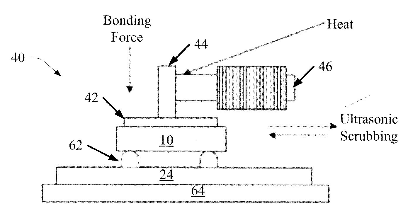
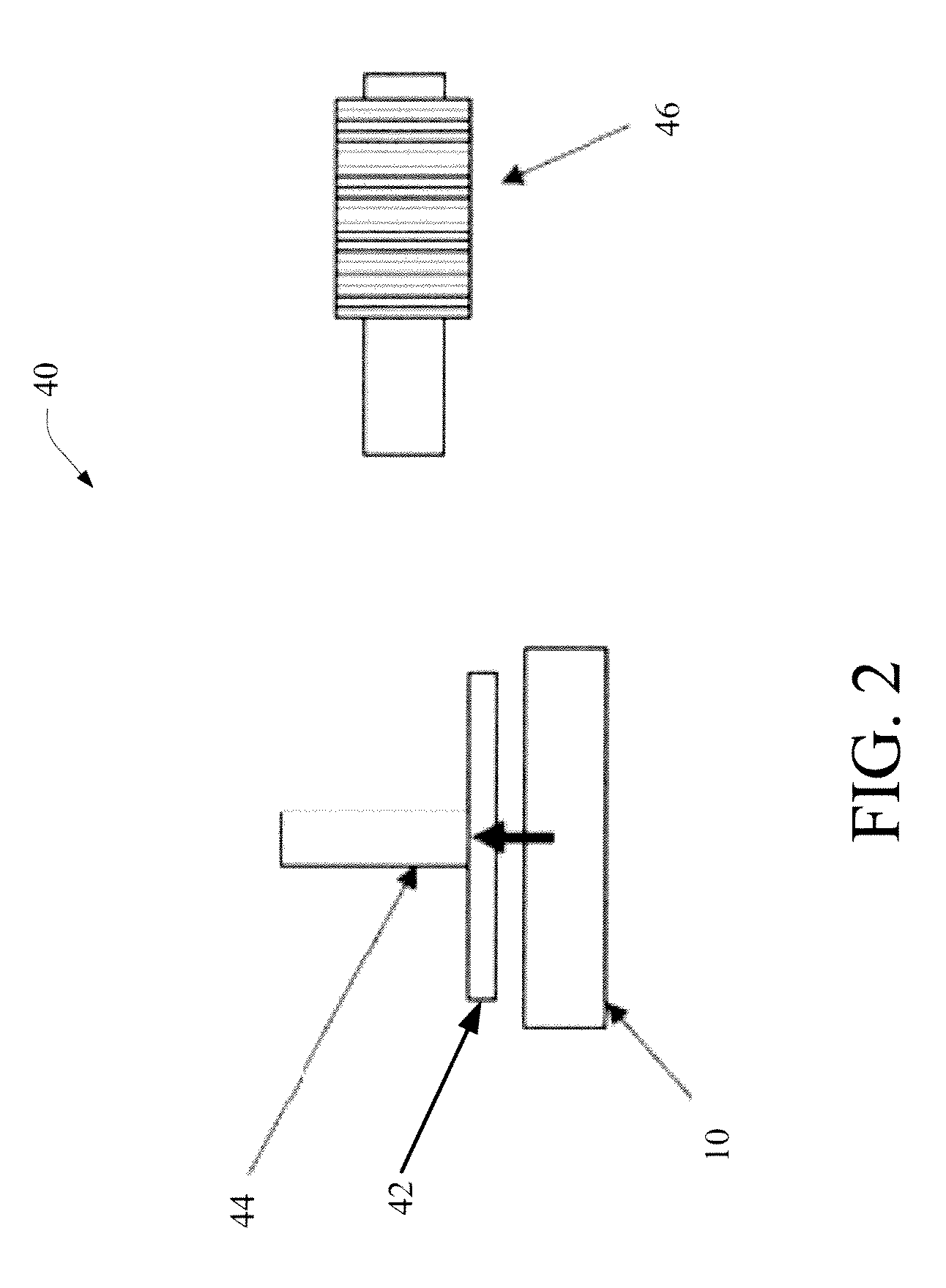
[0015]Systems and methods are described herein, which facilitate reducing or eliminating excess die attachment material accrual and parasitic conductive paths formed in conjunction therewith by locally melting a die attachment material (e.g., solder) using a combination of localized heat sources and ultrasonic energy. The heat sources bring the die attachment material close to its melting point, which reduces an amount of bonding force required of purely ultrasonic bonding techniques. An ultrasonic transducer brings the die attachment material the rest of the way up to its melting point, which reduces the overall temperature that the die and / or sensitive components thereon endure during the bonding process.

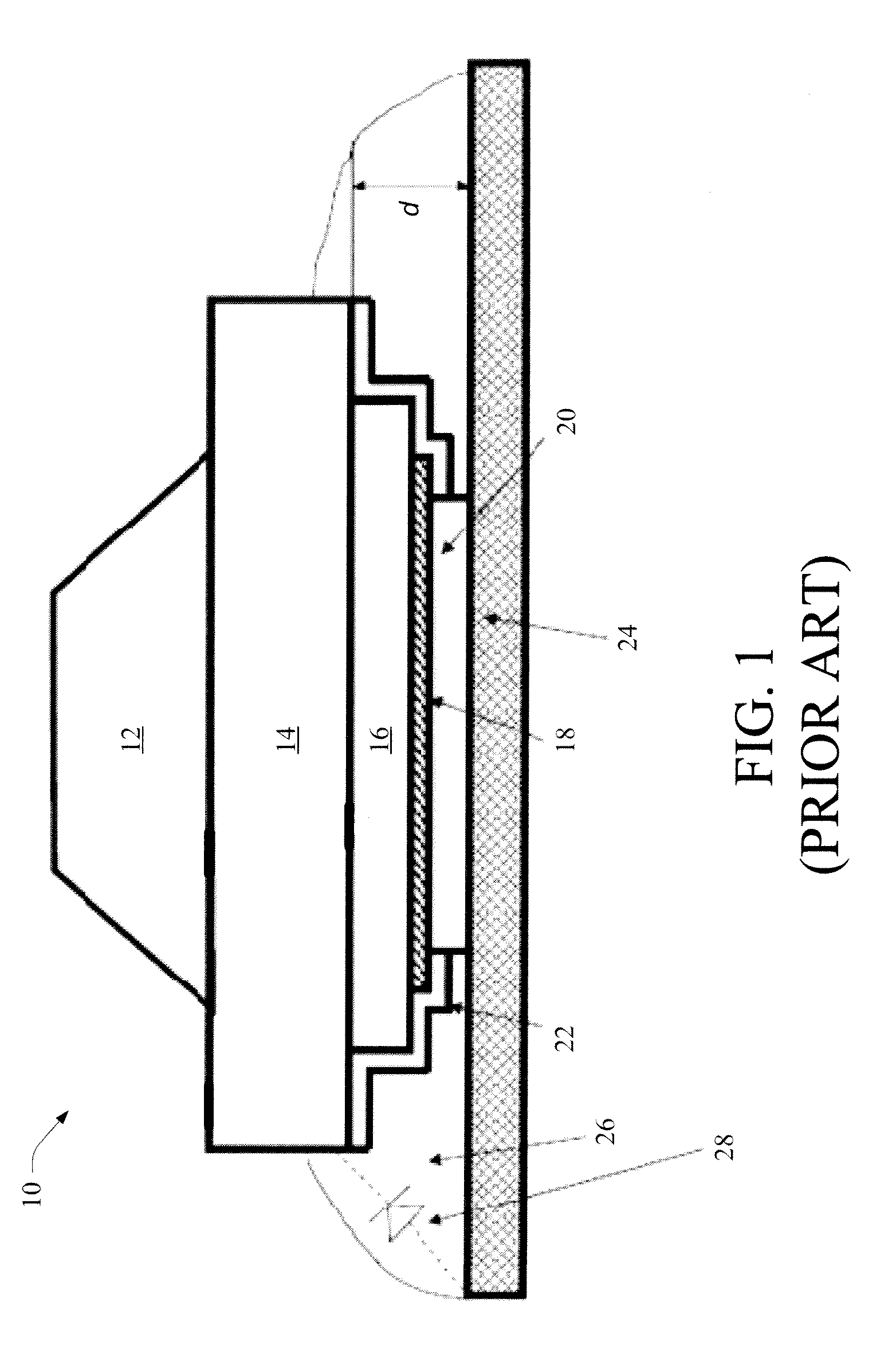
[0016]With reference to FIG. 1, a known die structure 10 is formed of multiple layers, including an LED layer 12 that overlays a silicon carbide (SiC) layer 14. The LED layer can comprise one LED or a plurality thereof. The SiC layer 14 overlays an epitaxial layer 16, which in tur...


PUM

PropertyMeasurementUnit
temperatureaaaaaaaaaa

Abstract

Systems and methods are provided to mitigate excess die attachment material accrual, and parasitic conductive paths formed thereby. A die attachment material (e.g., solder) is melted using a combination of localized heat sources and ultrasonic energy. The heat sources bring the die attachment material close to its melting point, which reduces an amount of bonding force associated with purely ultrasonic bonding techniques. An ultrasonic transducer brings the die attachment material the rest of the way up to its melting point, which reduces the overall temperature that the die and / or sensitive components thereon endure during the bonding process.

Description

BACKGROUND[0001]The subject innovation relates generally to die bonding systems and processes. It finds particular application in conjunction with light emitting diode (LED) dies, and will be described with particular reference thereto. However, it is to be appreciated that the systems and methods described herein are also amenable to other applications.[0002]Conventional soldering die attachment processes (e.g., U.S. Pat. No. 6,222,207 B1; U.S. Pat. No. 6,593,160 B2) have limitations concerning flip chip bonding of LED vertical dies (e.g., such as Cree XB dies based on SiC substrates). Close proximity of the edge of the SiC substrate to metal on the bottom of the die can cause conductive path if residual die attachment material (such a solder) extends up the edge of the die and contacts the SiC (FIG. 1). Similar problems are experienced when a predefined pattern of conductive die attachment material (e.g., silver (Ag) filled epoxy) is used for flip chip bonding. When force is appli...

Claims


Application Information

Patent Timeline
Patent Type & Authority Applications(United States)
IPC IPC(8): H01L21/60B23K1/06
CPCB23K20/023B23K20/10H01L2924/12032H01L2924/12041H01L2924/01074H01L24/81H01L2224/16H01L2224/81801H01L2924/01029H01L2924/01079H01L2924/01082H01L2924/3011H01L2924/01005H01L2924/01006H01L2924/01019H01L2924/01033H01L2924/01047H01L2924/0105H01L2924/00H01L2224/1134H01L2224/13144H01L2924/00014
Inventor KOLODIN, BORISGAO, XIANGELIASHEVICH, IVANWEAVER, JR., STANTON E.
Owner GE LIGHTING SOLUTIONS LLC
Why Eureka
Try Eureka