Method for improving surface plasmon resonance by using conducting metal oxide as adhesive layer

a technology of conducting metal oxide and surface plasmon, which is applied in the field of biochemical tests and gas detection, can solve the problems of lowering the sensitivity and reliability of the spr sensor chip, not good for optical properties, and so as to achieve a large reduction of sensitivity and competitiveness, lowering the sensitivity and reliability of the sensor chip, and high competitiveness

Active Publication Date: 2009-06-25
NAT TAIWAN UNIV
View PDF1 Cites 22 Cited by
  • Summary
  • Abstract
  • Description
  • Claims
  • Application Information

AI Technical Summary

Benefits of technology

[0007]In traditional SPR sensor chips, a gold film of 50 nm thick is fixed onto a glass substrate, and thus a highly active metal including chromium (Cr) or titanium (Ti) of several nanometers used as a chip adhesive layer is developed to increase the adhesive force between the gold film and the glass, but when the thickness of this type of opaque material is up to 5 nm, the incident light will be reflected completely. Although only 1-2 nm of chromium (Cr) or titanium (Ti) was usually plated, such arrangement is obviously not good for the optical property, and has the disadvantage of lowering the sensitivity and reliability of the SPR sensor chip.
[0008]Biochips used for analyzing the immunity of biomolecules or sensor chips used for detecting the concentration of a gas should take the size (in a micro scale or even a nano scale) of the sensing object into consideration, and thus the sensitivity of a system is a key index for the application and development of excellent sensors with high competitiveness and reliability is the key. In view of the opaqueness of the intermediate layer made of chromium or titanium metal and used in the manufacturing process of a traditional SPR biochip, the sensor chip greatly lowers the sensitivity and reliability of the sensor chip, even though the adhesive force between the nano gold thin film and the chip header. On the other hand, the sensitivity is lowered greatly, and thus the inventor's research team aims at the aforementioned problem to provide an electron transfer mechanism that adopts specially processed indium tin oxide and zinc oxide thin film between the gold film layers to replace the traditional adhesive layer made of chromium. The invention further improve the SPR curve by using indium tin oxide and zinc oxide thin films to progress the light transmission rate and provide a stable adhesive force in addition, so as to enhance the sensitivity and detection efficiency of the sensors.
[0009]The conducting metal oxide nano thin film replaces the traditional high-activity metal thin film adhesive layer, not only solving the adverse infection of the opaque chromium or titanium thin film on the sensitivity of detecting a surface by a SPR chip, but also exciting the activating zinc oxide thin film by the electron transfer mechanism to emit lights as well as synchronously strengthening the surface plasmon resonance (SPR). By applying the conducting metal oxide nano thin film to the biomedical sensing system, and detecting the combining condition of specific biomolecules or gas molecules in the microchannels on the surface of the biomedical chip in accordance with the detection principle of SPR, we can obtain a more sensitive, reliable and practical gas and biomolecule detector that can be more applicable for future developments of multi-channel high throughput detection and high sensitivity portable instruments. The present invention concurrently achieves the effects of high sensitivity and high throughput.

Problems solved by technology

Although only 1-2 nm of chromium (Cr) or titanium (Ti) was usually plated, such arrangement is obviously not good for the optical property, and has the disadvantage of lowering the sensitivity and reliability of the SPR sensor chip.
In view of the opaqueness of the intermediate layer made of chromium or titanium metal and used in the manufacturing process of a traditional SPR biochip, the sensor chip greatly lowers the sensitivity and reliability of the sensor chip, even though the adhesive force between the nano gold thin film and the chip header.

Method used


Image

  • Method for improving surface plasmon resonance by using conducting metal oxide as adhesive layer
  • Method for improving surface plasmon resonance by using conducting metal oxide as adhesive layer
  • Method for improving surface plasmon resonance by using conducting metal oxide as adhesive layer

Examples


Embodiment Construction

[0025]The above and other objects, features and advantages of the present invention will become apparent from the following detailed description taken with the accompanying drawing.

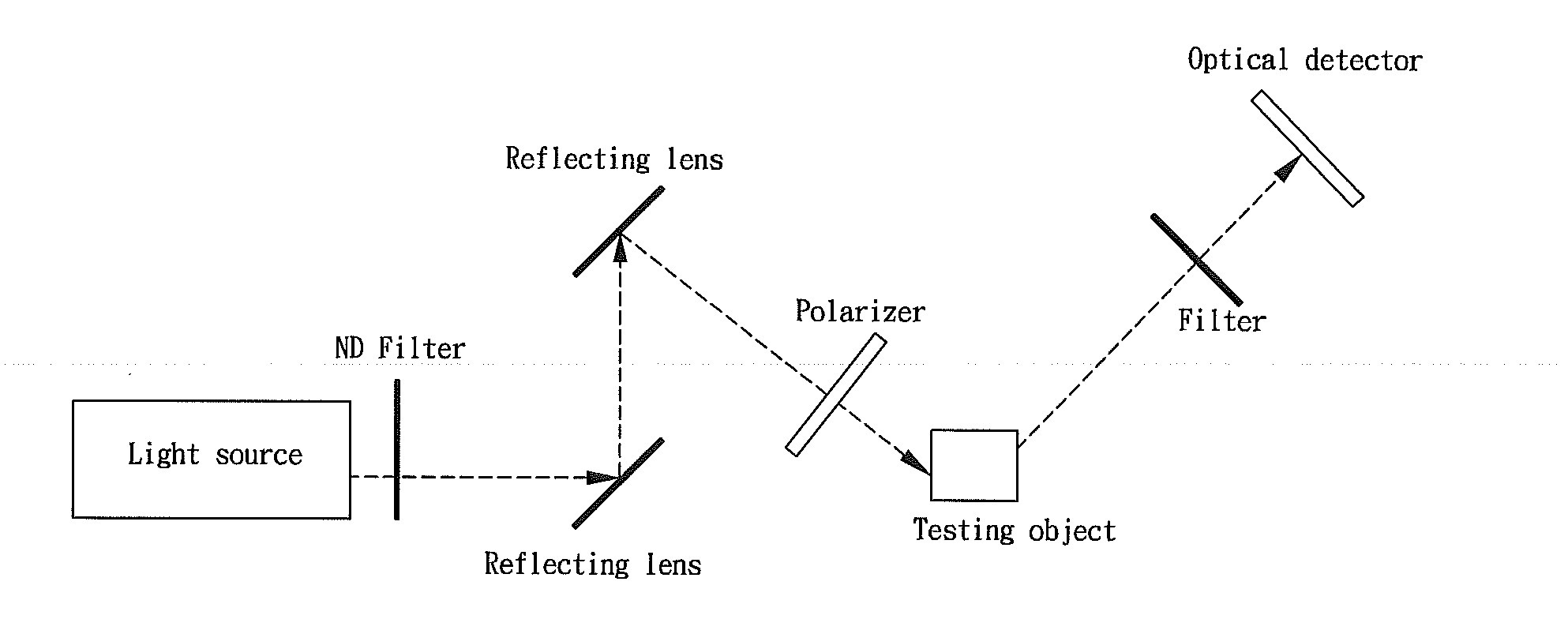
[0026]Principle of Measuring Surface Plasma Wave and Evanescent Wave

[0027]Metal is a conductor filled with free electrons inside. If these electrons are excited by an appropriate variable electric field to produce surface plasmon oscillations and propagated in a waveform along a surface (which is an interface of a metal and a certain dielectric material), and that is a surface plasma wave (SPW or SEW). This phenomenon was discovered by R. W. Wood in the 20th Century during his research on diffractions of a metal surface.

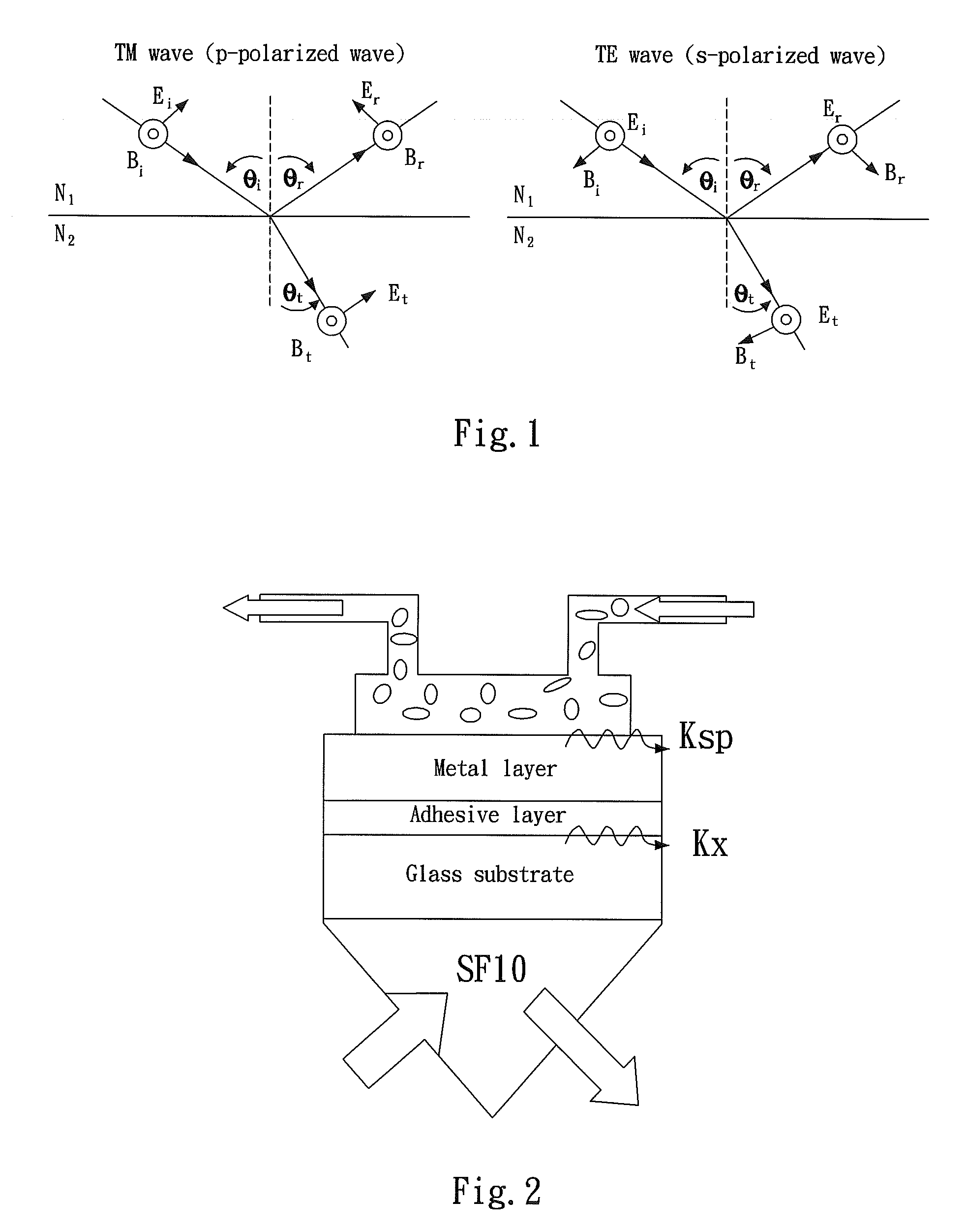
[0028]The aforementioned variable electric field must include a p-polarized light having TM waves, and the vibration direction of its electric field is parallel to the incident plane, and the light is incident into a prism (or a coupler) with an angle greater than the critical angle. In th...


PUM

PropertyMeasurementUnit
thicknessaaaaaaaaaa
wavelengthaaaaaaaaaa
incident angleaaaaaaaaaa

Abstract

Surface plasmon resonance (SPR) sensing technique which provides high specificity and accuracy has been an important method for molecular sensing technology. In the past, in order to affix 45 nm gold film onto glass or silicon substrate, several nanometers of chromium (Cr) or titanium (Ti) has been used as adhesive layer for the attachment of Au film. However, the existence of Cr or Ti thin film deteriorates the performance of SPR sensor due to their characteristic optical absorption. Our experimental results have confirmed the uses of conducting metal oxide, specifically, ITO and Zinc Oxide (ZnO) can be used to replace Cr or Ti for better performance in terms of SPR resonant properties (resonant angle and HMBW) and sensitivity enhancement for 3 to 15 times than traditional ones. It would contribute significantly to the SPR applications in both biosensors and gas sensors.

Description

FIELD OF THE INVENTION[0001]The present invention relates to a method for biochemical tests and gas detections, and more particularly to a method that uses surface plasmon resonance (SPR) for the detection.BACKGROUND OF THE INVENTION[0002]Biochip becomes increasingly popular in academic, government and private organizations in different countries. For DNA chips, technologies related to DNA binding analysis, sequence detection, quantitative analysis, capillary electrophoresis separation detection, nucleic acid amplification and parallel gene expression analysis become well developed. In the meantime, a series of other analytic methods such as cell separation, cell immunity analysis, and applications integrated with combinatorial chemistry are derived, and the research and development of new medicines to provide a high throughput screening. In addition, material technologies are well developed, and biochips are not only made of silicon, but also made of plastic films and elastomers as...

Claims


Application Information

Patent Timeline
Patent Type & Authority Applications(United States)
IPC IPC(8): G01N21/55
CPCG01N21/553
Inventor LIN, CHII-WANNCHIU, NAN-FUFENG, WEI-YICHANG, CHIA-CHENHO, KUO-CHUANLEE, CHIH-KUNGWU, KUANG-CHONG
Owner NAT TAIWAN UNIV
Why Eureka
Try Eureka