

Dry etching equipment and method for producing semiconductor device
a technology of dry etching and semiconductors, which is applied in the direction of basic electric elements, electrical equipment, electric discharge tubes, etc., can solve the problem of difficult control of the critical dimension variation on the nanometer scale (cd)
- Summary
- Abstract
- Description
- Claims
- Application Information
AI Technical Summary
Benefits of technology
Problems solved by technology
Method used
Image

Examples
first embodiment
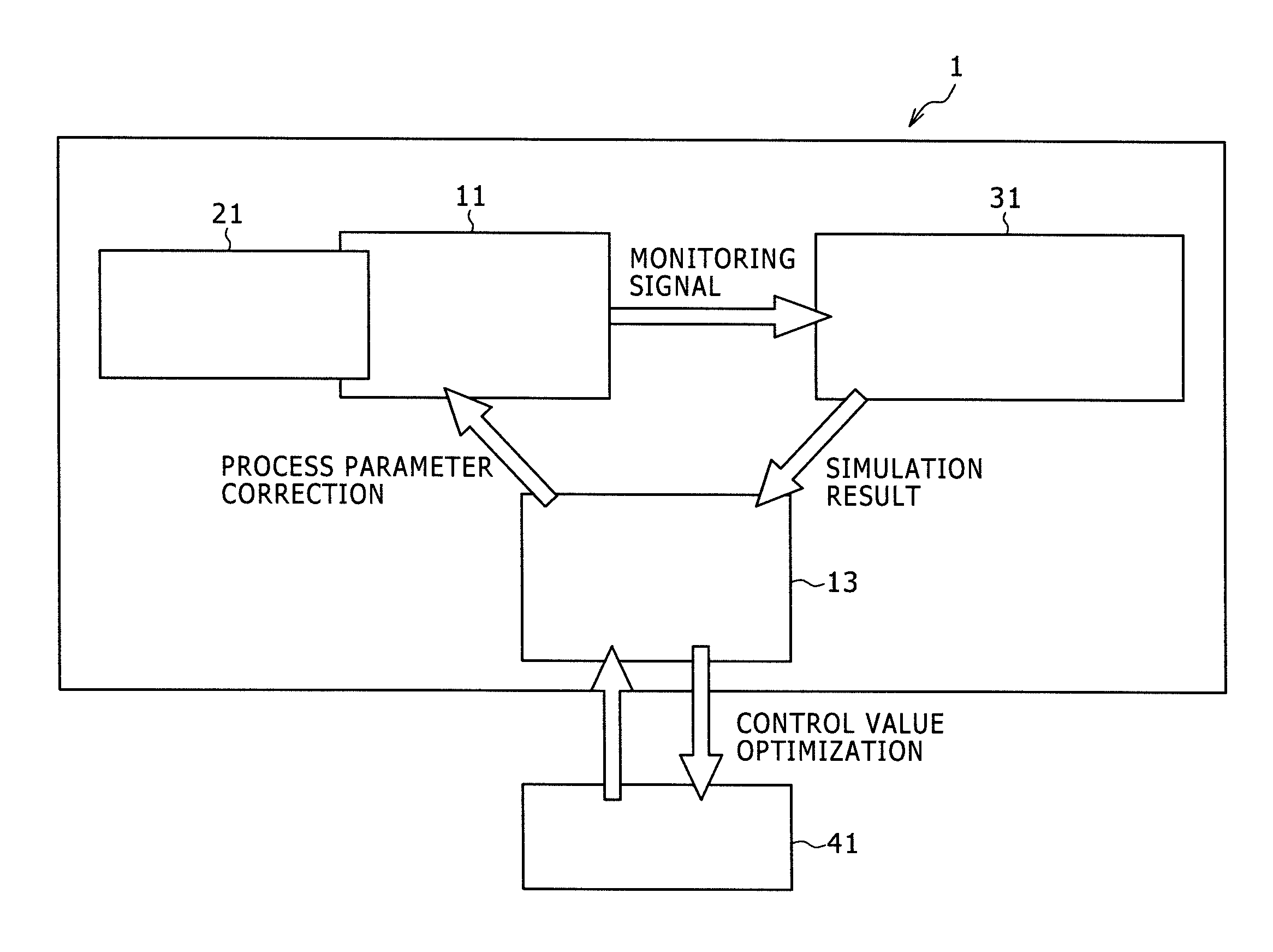
[0067]With respect to the etching by using the dry etching equipment 1 for various devices presumed to be produced, the topography simulation according to the algorithm of the topography simulator 31 in the first embodiment is described below with reference to FIG. 3.
[0068]Prior to the etching, a database for the topography simulator 31 is preliminarily prepared. The data shown below are merely an example and can be changed if desired.
[0069]Specifically, conditions are as follows.
With respect to the film thickness:[0070]Photoresist film thickness: 100 to 600 nm[0071]Antireflection coating film thickness: 50 to 100 nm[0072]Silicon film thickness: 40 to 300 nm
Photoresist width: 50 to 200 nm
With respect to the plasma conditions:[0073]Plasma density: 109 cm−2 to 1012 cm−3 [0074]Electron temperature: 0.5 to 7 eV[0075]Ion flux: 109 to 1017 cm−2 [0076]Radical flux: 109 to 1020 cm−2 [0077]Ion energy: 10 to 1,000 eV
With respect to the process parameter:[0078]Pressure: 0.13 to 67 Pa[0079]Gas ...
second embodiment
[0110]Next, in the case of conducing an etching by using the dry etching equipment 1, while presuming various devices to be produced, the topography simulation according to the algorithm of the topography simulator 31 in the second embodiment is described below with reference to FIG. 5.
[0111]In the second embodiment, a computer allowing high-speed processing is used. For example, a computer which can achieve one or more correction feedbacks in a real time of 2 seconds is installed in or connected to the dry etching equipment 1 through a network (LAN using serial, Ethernet, or the like) so that they can communicate with each other. Topography simulation according to the algorithm in the first embodiment is performed in real time during etching. Therefore, unlike the first embodiment, there is no need to preliminarily prepare a digital database in the present second embodiment.
[0112]With respect to the light-emission data of plasma and the ion energy of plasma, as in the case of the f...
third embodiment
[0171]Next, in the case of conducting the etching by using the dry etching equipment 1, while presuming various devices to be produced, the topography simulation according to the algorithm of the topography simulator 31 in the third embodiment is described below with reference to FIGS. 11 and 12.
[0172]In the third embodiment, without using a plasma monitoring signal of the monitor 21 in the dry etching equipment 1 (plasma emission intensity or ion energy), a plasma vapor phase module (an example of the results of calculation for the distribution of flux and the change of flux with time is shown in FIGS. 9A and 9B) and a collisional sheath module (an example of the results of calculation for the distribution of ion energy and the distribution of ion incident angle is shown in FIGS. 10A and 10B) are linked to the topography simulator 31, and the whole phenomenon from the vapor phase to the surface is modeled to estimate a critical dimension (CD), thereby correcting a process parameter...
PUM
| Property | Measurement | Unit |
|---|---|---|
| Time | aaaaa | aaaaa |
| Solid angle | aaaaa | aaaaa |
Abstract
Description
Claims
Application Information