
Semiconductor integrated circuit and method for testing the same

a technology of integrated circuits and semiconductors, applied in the direction of liquid/fluent solid measurement, power supply for data processing, instruments, etc., can solve the problems of increasing test costs, difficult to ensure high-quality test, increasing power consumption of combinational circuits, etc., to reduce test time, reduce test costs, and reduce power consumption

Inactive Publication Date: 2009-06-25
SOCIONEXT INC
View PDF11 Cites 8 Cited by
  • Summary
  • Abstract
  • Description
  • Claims
  • Application Information

AI Technical Summary

Benefits of technology

[0027]It is therefore an object of the present invention to effectively reduce power consumption during shift operation in scan testing and in logic BIST without increasing the circuit area and without adversely affecting the speed of performing function.
[0028]In order to achieve the above object, the present invention employs a structure in which only power supply voltage to a combinational circuit can be lowered during shift operation in scan testing and in logic BIST, thereby reducing power consumption in the combinational circuit.
[0051]In the inventive semiconductor integrated circuits and the inventive test methods, during shift operation in scan testing, the power supply voltage to the combinational circuit is cut off or set to a lower voltage as compared with capture operation, thereby effectively suppressing the amount of power consumed by the combinational circuit during the shift operation. If, during the shift operation, the power supply voltage to the flip flop circuits is set to a higher voltage as compared with capture operation, the shift operation by the flip flop circuits is performed at higher speed, thereby effectively reducing the test time.
[0052]In the present invention, the reduction in the power consumed by the combinational circuit during the shift operation, and the reduction in the test time are achieved just by lowering the power supply voltage to the combinational circuit and by raising the power supply voltage to the flip flop circuits. Therefore, unlike in the conventional circuits and conventional test methods, these advantages can be obtained without increasing the circuit area or decreasing the operating speed. In addition, since the power to the combinational circuit is cut off during shift operation, it is possible to reduce not only the amount of power consumed by the switching operation by the transistor in the combinational circuit, but also the amount of power consumed by leakage current occurring in the CMOS transistor being in a static state. Such leakage current is caused by the thinning of the gate insulating film of the transistor and has been arising as a problem recently.
[0053]Also, according to one embodiment of the present invention, an intermediate-potential prevention circuit prevents the input terminals of the flip flop circuits from having an intermediate potential while the power supply voltage to the combinational circuit is cut off, thereby effectively preventing excessive leakage current flow in, and damage to, the combinational circuit.
[0054]Moreover, according to one embodiment of the present invention, during shift operation in scan testing, the power supply voltage to the combinational circuit is lowered or cut off, or the power supply voltage to the flip flop circuits is raised, whereby the power consumption is reduced, or the test time is shortened. Then, supply of a clock signal to the flip flop circuits is stopped only for a certain period of time before the following capture operation is performed, thereby providing a certain waiting time before the capture operation. The presence of waiting time allows the combinational circuit and the flip flop circuits to operate in normal operation mode with normal power supply voltage being supplied, whereby stable test on the combinational circuit is ensured.

Problems solved by technology

However, as the number of devices in a semiconductor circuit has increased, the amount of time required to test the circuit has increased.
As a result, the test cost has been increasing.
In addition, since current semiconductor circuits provide high-performance and high-speed operation, it has become difficult to assure high-quality test.
Furthermore, as technology for microscaling semiconductor fabrication processes has progressed, operation of a system-on-a-chip is adversely affected by small defects, which did not cause any problems before.
High-resistance vias, short circuits, crosstalk, and other defects have manifested themselves as delay faults.
Since the running cost of an LSI tester is very high, if the tester is used for a long time, the final manufacturing cost of the semiconductor integrated circuit will be affected significantly.
However, in scan test or logic BIST conducted in a semiconductor integrated circuit including numerous devices, high-speed shift operation of the scan chain formed for testing many blocks in the semiconductor integrated circuit causes the semiconductor integrated circuit to consume a significant amount of power, such that normal operation and thus appropriate test cannot be performed.
At this time, many transistors within the combinational circuit simultaneously perform switching, thereby momentarily consuming a considerable amount of power.
In these conventional techniques, power consumption can be suppressed, but penalties are likely to occur in the circuit area and the speed of performing function.
Therefore, the conventional flip flop circuits shown in FIGS. 30 and 31, which are capable of suppressing power consumption, have disadvantages in that the circuit area increases and the operation speed decreases.

Method used


Image

  • Semiconductor integrated circuit and method for testing the same
  • Semiconductor integrated circuit and method for testing the same
  • Semiconductor integrated circuit and method for testing the same

Examples


first embodiment

[0087]Hereinafter, a semiconductor integrated circuit and a method for testing the same according to a first embodiment of the present invention will be described.

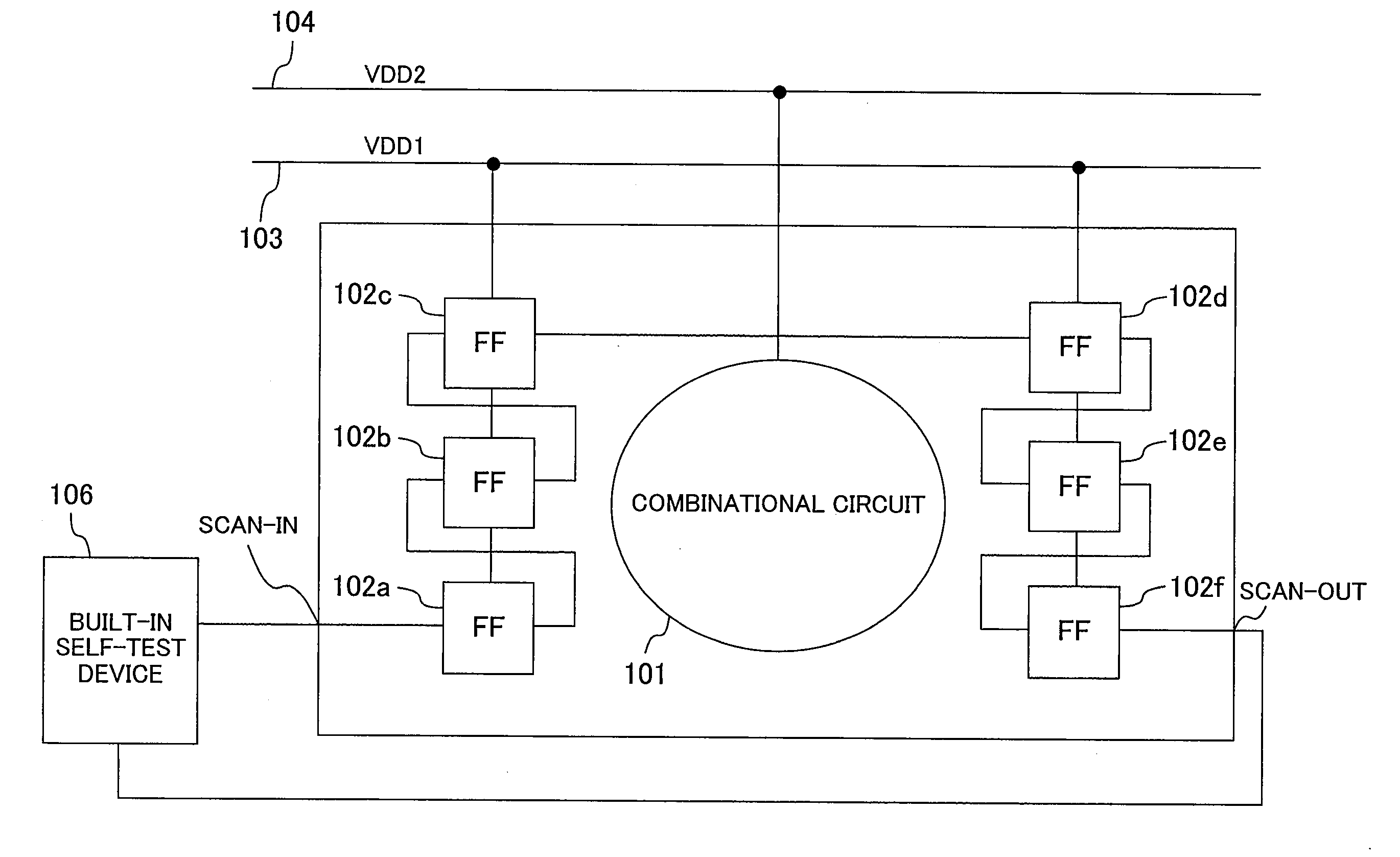
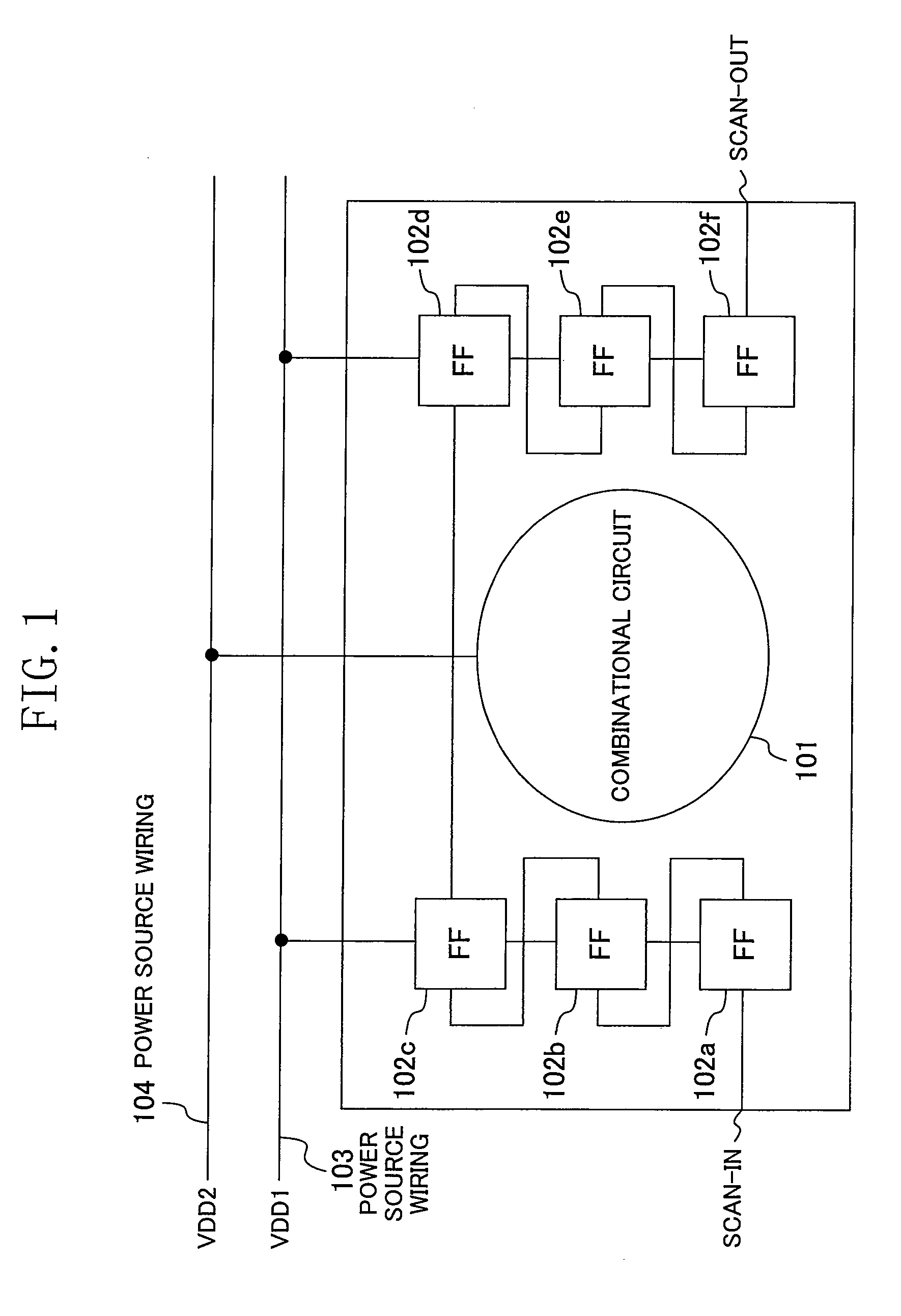
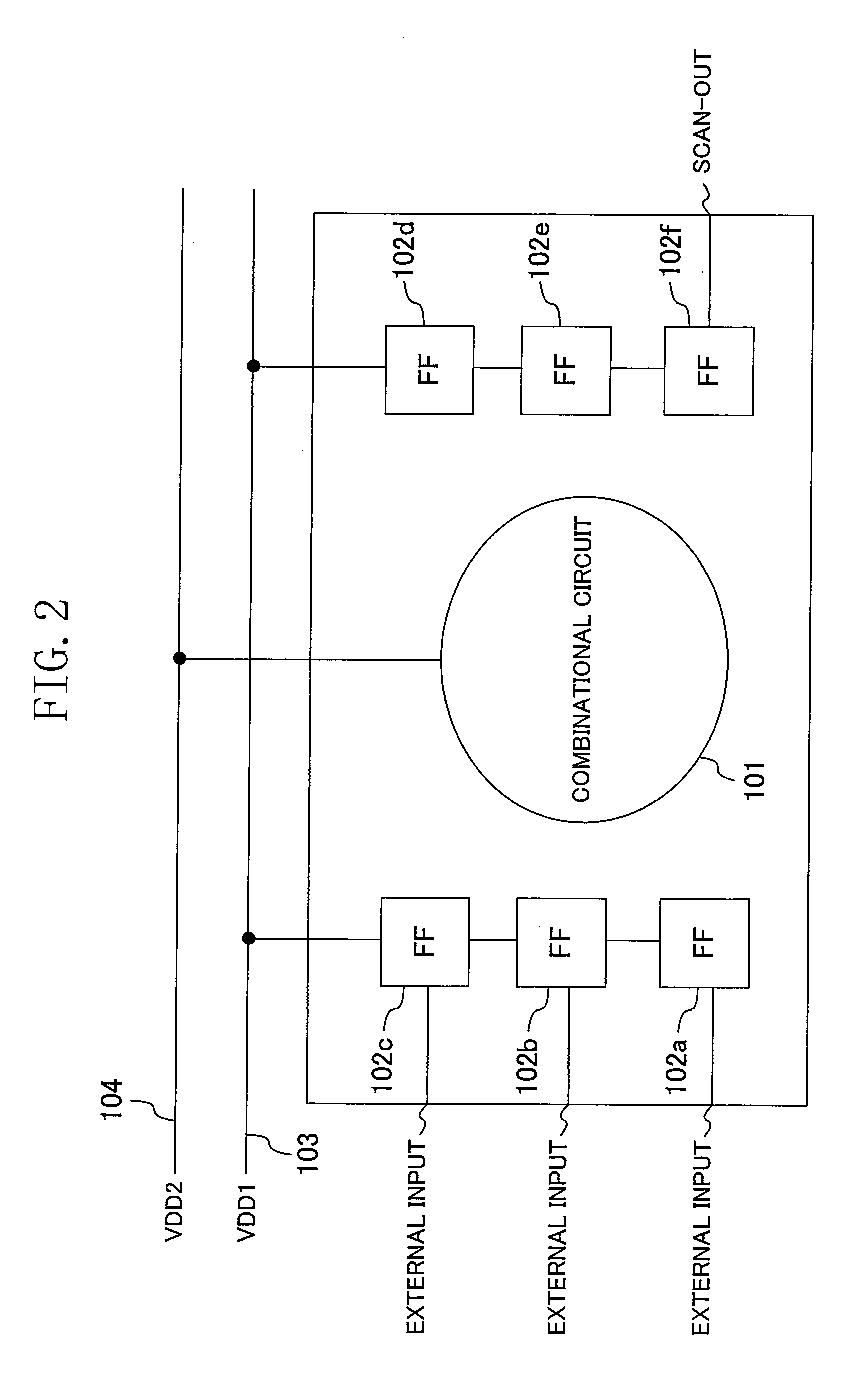
[0088]FIG. 1 is a circuit diagram illustrating the configuration of the semiconductor integrated circuit of the first embodiment. In FIG. 1, the reference numeral 101 denotes a combinational circuit. The reference numerals 102a to 102f indicate flip flop circuits. The reference numeral 103 refers to flip-flop-circuit power source wiring for supplying power supply voltage to the flip flop circuits 102a to 102f, while the reference numeral 104 represents combinational-circuit power source wiring for supplying power supply voltage to the combinational circuit 101. The power source wiring 103 and the power source wiring 104 are separate from, and function independently of, each other, such that the power source wiring 103 can apply a power supply voltage VDD1 to the flip flop circuits 102a to 102f, and the power source wiring ...

second modified example

of the First Embodiment

[0096]A typical semiconductor integrated circuit is not always designed so as to be capable of withstanding high-speed shift operation when the power supply voltage for normal operation is applied to the semiconductor integrated circuit. Even so, since the semiconductor integrated circuit of FIG. 1 is configured so that during shift operation, a voltage higher than that supplied in normal operation can be applied only to the flip flop circuits, the shift operation can be performed at high speed.

[0097]FIG. 5A indicates a test method for realizing the above-described high-speed shift operation. The test method shown in FIG. 5A includes four steps 205 to 208. In the first step 205, the power supply voltage to the flip flop circuits is raised. In the second step 206, test data is set in the flip flop circuits. In the third step 207, the power supply voltage to the flip flop circuits is lowered. In the fourth step 208, the combinational circuit is operated. By perf...

third modified example

of the First Embodiment

[0099]In the semiconductor integrated circuit of the first embodiment, the two power supply voltages VDD1 and VDD2 may be supplied from devices external to the semiconductor integrated circuit, or may be supplied by a variable power supply circuit included in the semiconductor integrated circuit. FIG. 7 illustrates a semiconductor integrated circuit provided with a variable power supply circuit. In FIG. 7, the reference numeral 105 denotes the variable power supply circuit.


PUM


Abstract

In a semiconductor integrated circuit, power source wiring for supplying power supply voltage to a plurality of flip flop circuits, and power source wiring for supplying different power supply voltage to a combinational circuit are provided individually, so that the power supply to the flip flop circuits and the power supply to the combinational circuit can be performed separately from, and independently of, each other. During shift operation in scan testing, the power supply voltage to the combinational circuit is set to a low voltage or cut off, thereby suppressing the amount of power consumed by the combinational circuit portion during the shift operation. At the same time, the power supply voltage to the flip flop circuits is set to a high voltage during the shift operation.

Description

CROSS-REFERENCES TO RELATED APPLICATIONS[0001]This Non-provisional application claims priority under 35 U.S.C. §119(a) on Patent Application No. 2005-24149 filed in Japan on Jan. 31, 2005, the entire contents of which are hereby incorporated by reference.BACKGROUND OF THE INVENTION[0002]The present invention relates to semiconductor integrated circuits and methods for testing the same.[0003]In recent years, progress in technology for microscaling semiconductor fabrication processes has continued without a letup, and the semiconductor technology has consequently moved into the era of the 90 nm and 65 nm generations. This progress has enabled a complex system conventionally composed of a plurality of LSIs to be integrated on a single silicon chip and realized as a system-on-a-chip. Since transistor integration per unit area and operating frequency have been increased rapidly, a plurality of IP cores having different functions and features can be incorporated into a single chip, thereb...

Claims


Application Information

Patent Timeline
Patent Type & Authority Applications(United States)
IPC IPC(8): G01R31/3177G06F11/25G01R31/3187
CPCG01R31/318575
Inventor ISHIMURA, TAKASHITAKEOKA, SADAMI
Owner SOCIONEXT INC
Learn More