Monolithic light emitting device and driving method therefor

Inactive Publication Date: 2009-07-02
SUMITOMO CHEM CO LTD
View PDF8 Cites 10 Cited by
  • Summary
  • Abstract
  • Description
  • Claims
  • Application Information

AI Technical Summary

Benefits of technology

[0010]The present invention has another object of providing a monolithic light emitting device being excellent in color tone stability, capable of controlling color tone, and suitable for miniaturizing, a lighting device including the same and a driving method therefor.

Problems solved by technology

The conventional method of producing white light emitting devices and white light emitting diodes including a nitride semiconductor is as described above, thus, the method is complicated, a special production apparatus is required for maintaining assembly accuracy and quantification precision in the steps of the method, and additionally, checks for every steps are also necessary, leading to a necessity of large equipment investment generating correspondent production cost.
However, since the light emitting diode device has small chip size, handling thereof is difficult.
As a result, an expensive high precision handling machines is required, and additionally, it is difficult to scale down the chip size of the light emitting diode device at our disposal, thus, cost saving is difficult.

Method used


Image

  • Monolithic light emitting device and driving method therefor
  • Monolithic light emitting device and driving method therefor
  • Monolithic light emitting device and driving method therefor

Examples


example 1

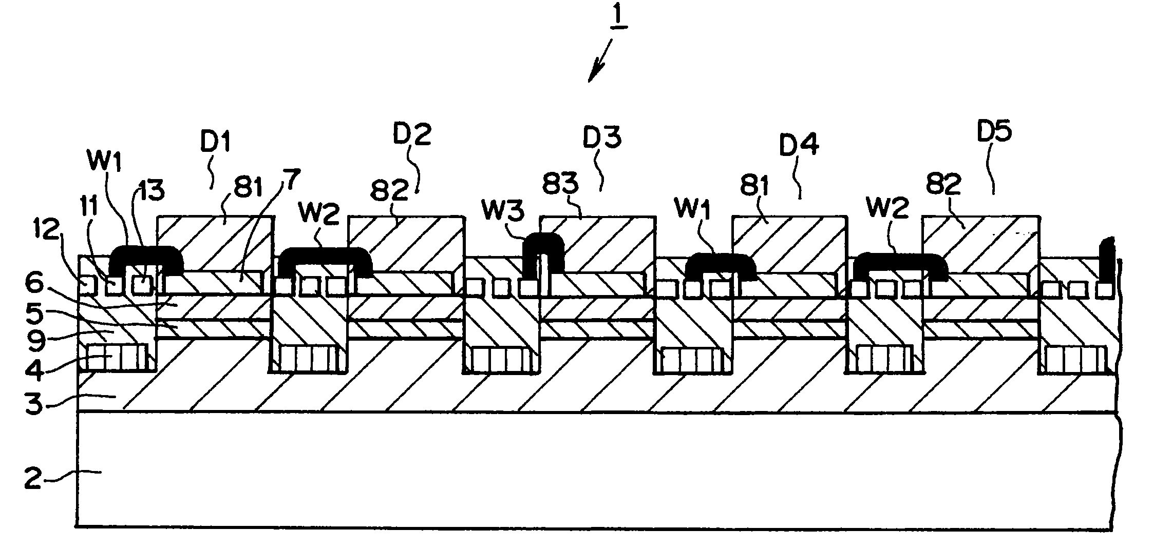
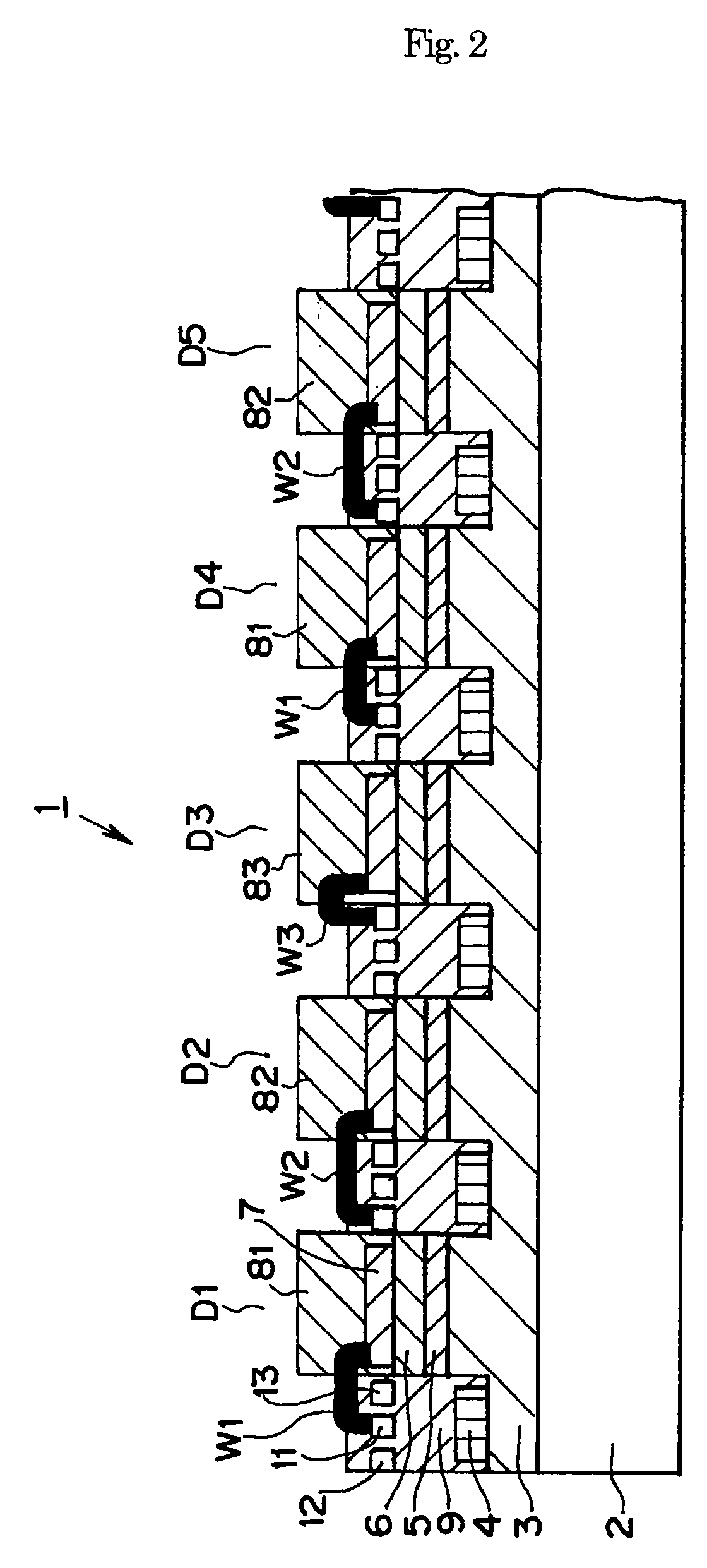
[0150]Sapphire having C-plane mirror-polished was used as a substrate. Crystal growth was carried out by MOVPE. An n-type GaN layer was grown by a two-step growth using low temperature-growing GaN as a buffer layer. InGaN well layer and non-doped GaN barrier layer are grown alternately to form a multi quantum well structure, and a Mg-doped p-type layer was grown.

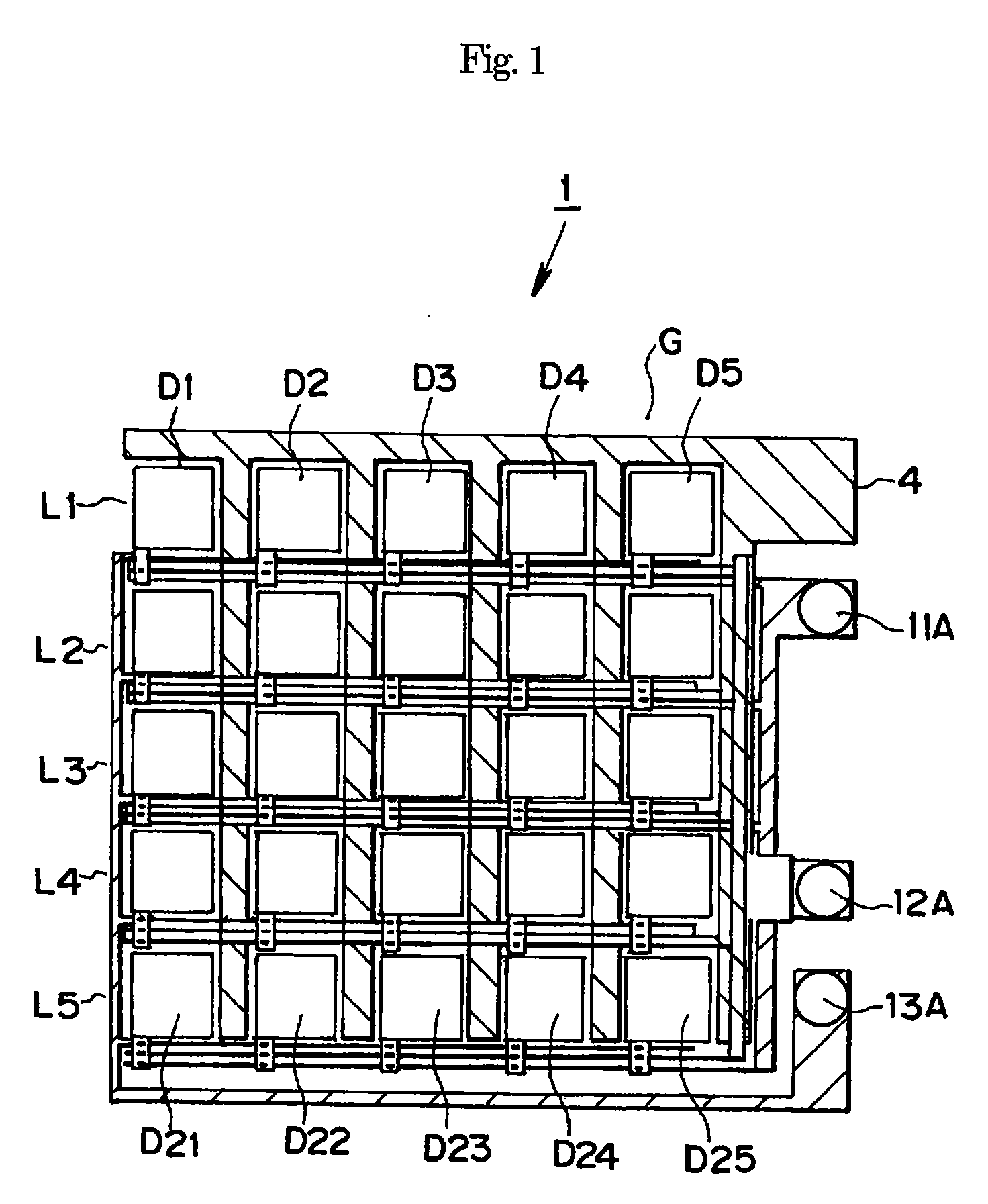
[0151]A Ni—Au transparent electrode was formed on the resultant by an ordinary method to obtain a light emitting diode (hereinafter, abbreviated as LED). Al was used as the n electrode. Further, by repeating the photolithographic steps as described in the embodiment, a device including an array of 3×3 as shown in FIG. 17 was produced. One pixel has a size of 100 μm×100 μm. The device was tested. It was confirmed pixels of 1 to 3 groups emitted lights. FIGS. 18 to 20 were stereomicrographs in device operation. Thereafter, viscous liquid prepared by mixing a phosphor (terbium.aluminum.garnet) and ultraviolet-hardening resin wa...


PUM


Abstract

A monolithic light-emitting device and driving method therefore includes a plurality of light-emitting diodes, array-arranged monolithically on a single substrate. Thie light-emitting diodes include a pn junction-containing semiconductor material and a phosphor-containing layer passing light emitted from the semiconductor material, absorbing part, or whole of the light for conversion into light having a different wavelength. The array is constituted of a light-emitting diode group consisting of m (m≧2) pieces of the light-emitting diode, the light emitting diode group being constituted of N types (N≧2, providing N≦m) of light-emitting diodes, each having either one of preset N types of light-emitting spectrum patterns. An average light-emitting spectrum from the whole array can be changed by regulating a power supplied to the light-emitting diodes for each light-emitting diode group sorted according to the type of the light-emitting spectrum pattern.

Description

TECHNICAL FIELD[0001]The present invention relates to a monolithic light emitting device, a lighting comprising the same, and a driving method therefor.BACKGROUND ART[0002]White light emitting diodes including a nitride semiconductor are used widely as a light source for backlight of small liquid crystal display such as cellular phone, and an application as a light source is expected instead of fluorescent lamps from now on. For replacing fluorescent lamps with white light emitting diodes, cost saving is an important problem together with improvement in luminous efficiency. Furthermore, in new technology such as micro machine and capsule type gastric camera, demand for micro lighting is expected to rapidly grow in the future.[0003]White light emitting devices and white light emitting diodes including a nitride semiconductor often used recently are produced, for example, by the following process. First, an epitaxial wafer is subjected to processing such as etching and electrode evapo...

Claims


Application Information

Patent Timeline
IPC IPC(8): H01L33/00H01L33/32H01L33/06H01L33/36H01L33/50H01L33/54H01L33/56
CPCG02B6/0025G02B6/0046G02B6/0051H01L51/5036G02B6/0073H01L27/156H01L51/0007G02B6/0068H10K71/15H10K50/125F21S2/00H01L33/00
Inventor HIROYAMA, YUICHIHATA, MASAHIKOTSUCHIDA, YOSHIHIKO
Owner SUMITOMO CHEM CO LTD
Why Eureka
Try Eureka