Light-emitting device of group iii nitride-based semiconductor and manufacturing method thereof

a technology of nitride-based semiconductors and light-emitting devices, which is applied in the direction of semiconductor/solid-state device manufacturing, semiconductor devices, electrical devices, etc., can solve the problems of difficult to achieve a breakthrough in technology to minimize dislocation density, difficult to suppress thread dislocation, etc., and achieve the effect of increasing the light extraction efficiency of the light-emitting device and suppressing thread dislocation

Inactive Publication Date: 2009-07-02
ADVANCED OPTOELECTRONICS TECH
View PDF3 Cites 14 Cited by
  • Summary
  • Abstract
  • Description
  • Claims
  • Application Information

AI Technical Summary

Benefits of technology

[0014]The primary aspect of the present invention is to provide a light-emitting device of Group III nitride-based semiconductor and manufacturing method thereof. Due to lateral growth of the Group III nitride formed directly on a substrate, threading dislocations can be suppressed, and therefore the light extraction efficiency of the light-emitting device can be increased.

Problems solved by technology

The increase of acceptor concentration in a light-emitting layer (active layer) is difficult, and more difficult in a wide band gap gallium nitride layer.
In the meanwhile, due to the substantially large lattice match between a sapphire substrate and gallium nitride material, it's not easy to achieve a breakthrough in technology to minimize the dislocation density.
However, with larger contact area between two layers having different lattice constants and thicker accumulation of the atomic layers, the dislocation density caused by lattice mismatch becomes denser.

Method used


Image

  • Light-emitting device of group iii nitride-based semiconductor and manufacturing method thereof
  • Light-emitting device of group iii nitride-based semiconductor and manufacturing method thereof
  • Light-emitting device of group iii nitride-based semiconductor and manufacturing method thereof

Examples


Embodiment Construction

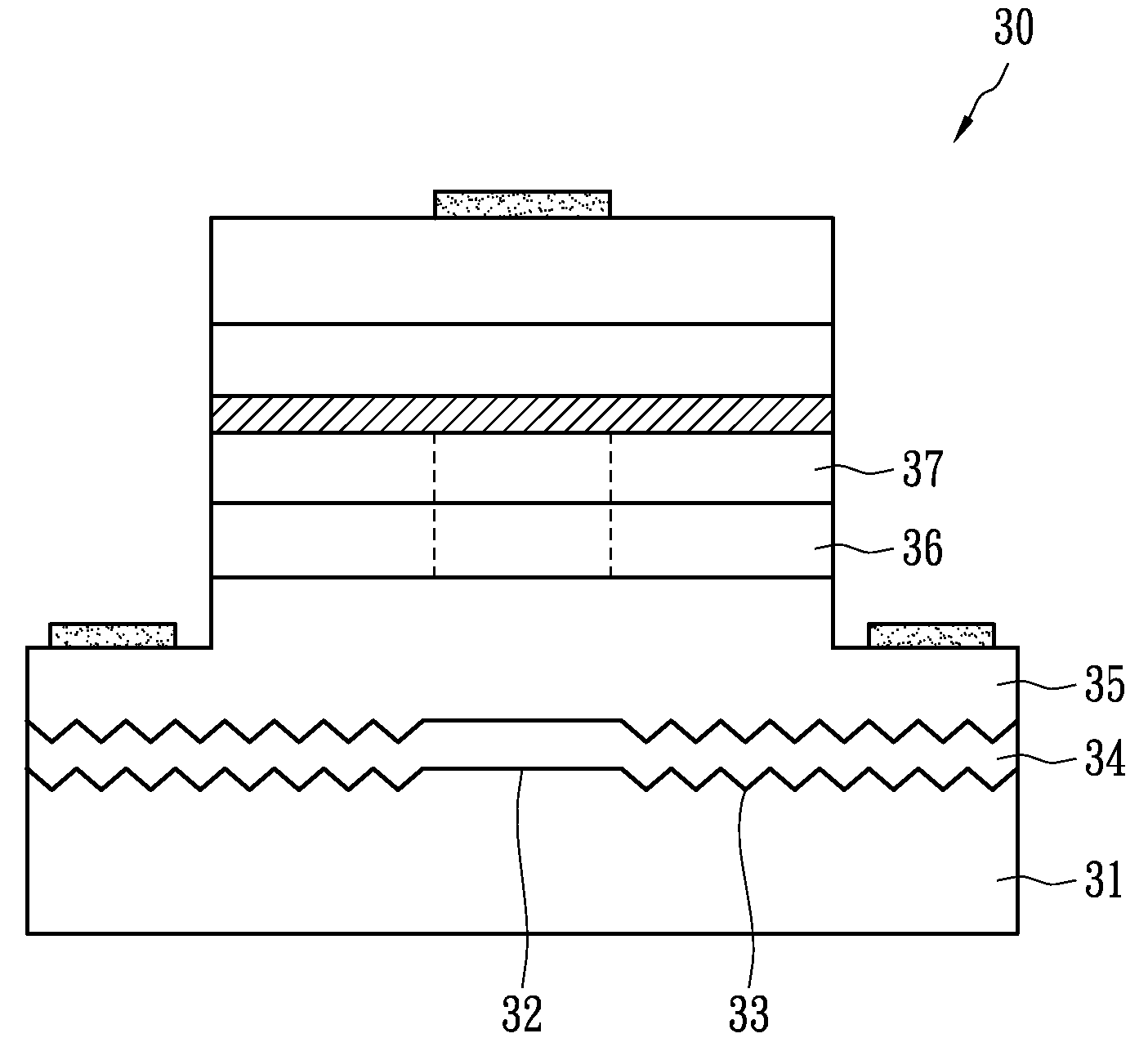
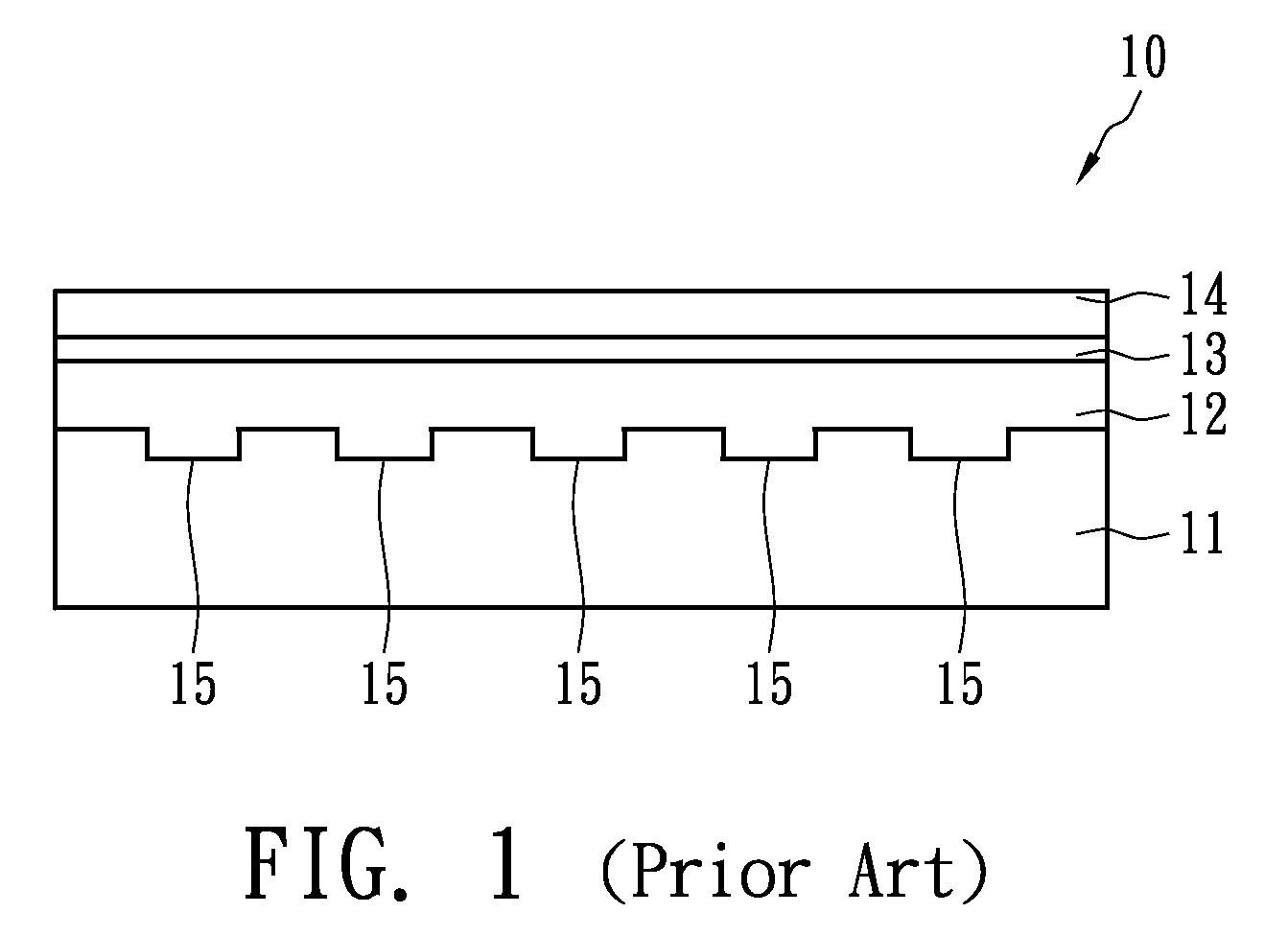
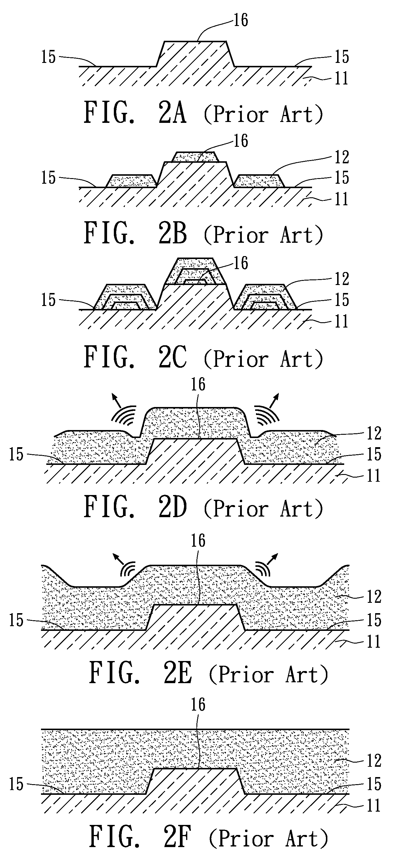
[0039]FIG. 7A is a cross sectional view illustrating a light-emitting device of Group III nitride-based semiconductor according to one embodiment of the present invention. The light-emitting device 70 comprises a substrate 71, a first buffer layer 721, a second buffer layer 722, an N-type semiconductor layer 73, an active layer 74 and a P-type semiconductor layer 75. Moreover, an N-type electrode 77 is formed on the N-type semiconductor layer 73 and a P-type electrode 76 is formed on the P-type semiconductor layer 75. The substrate 71 comprises a first surface 712, a plurality of convex portions 711 protruding from the first surface 712 and a second surface 713 opposite to the first surface 712. Each convex portion 711 is surrounded by a part of the first surface 712 as shown in FIG. 8(a).

[0040]The first buffer layer 721 is initially provided on the top surfaces of the convex portions 711, then extends laterally from these top surfaces, and finally connects mutually. The second buff...


PUM

PropertyMeasurementUnit
band gapaaaaaaaaaa
thicknessaaaaaaaaaa
heightaaaaaaaaaa

Abstract

A light-emitting device of Group III nitride-based semiconductor comprises a substrate, a first Group III nitride layer and a second Group III nitride layer. The substrate comprises a first surface and a plurality of convex portions protruding from the first surface. Each convex portion is surrounded by a part of the first surface. The first Group III nitride layer is jointly formed by lateral growth starting at top surfaces of the convex portions. The second Group III nitride layer is formed on the first surface, wherein a thickness of the second Group III nitride layer is less than a height of the convex portion. Moreover, the first Group III nitride layer and the second Group III nitride layer are made of a same material.

Description

BACKGROUND OF THE INVENTION[0001]1. Field of the Invention[0002]The present invention relates to a light emitting device (LED) of Group III nitride-based semiconductor and the manufacturing method thereof, and relates more particularly to a light-emitting device of Group III nitride-based semiconductor with high light extraction efficiency and the manufacturing method thereof.[0003]2. Description of the Related Art[0004]With widespread applications of light emitting devices in different products, the semiconductor materials used in making blue LEDs have in recent years been the focus of research in the opto-electronic materials and is device area. To date, blue LEDs are made of zinc selenide (ZnSe) material, silicon carbide (SiC) material and indium gallium nitride (InGaN) material, all of which are wide band gap semiconductors, with band gap values over approximately 2.6 eV. Gallium nitride is a direct, wide band gap semiconductor, and therefore it can produce high intensity of lig...

Claims


Application Information

Patent Timeline
Patent Type & Authority Applications(United States)
IPC IPC(8): H01L33/00H01L21/02H01L21/04
CPCH01L33/007
Inventor HUANG, SHIH CHENGTU, PO MINYEH, YING CHAOLIN, WEN YUWU, PENG YIHSU, CHIH PENGCHAN, SHIH HSIUNG
Owner ADVANCED OPTOELECTRONICS TECH
Why Eureka
Try Eureka