Semiconductor device and manufacturing method thereof

a technology of semiconductor devices and semiconductors, applied in semiconductor devices, diodes, electrical devices, etc., to achieve the effect of high avalanche resistan

Inactive Publication Date: 2009-07-02
PANASONIC CORP
View PDF12 Cites 149 Cited by
  • Summary
  • Abstract
  • Description
  • Claims
  • Application Information

AI Technical Summary

Benefits of technology

[0013]However, externally providing a diode increases the number of parts and also increases the occupied area, which is not preferable for semiconductor devices for which reduction in size and cost has been demanded.
[0014]The present invention is made to solve the above problems and it is an object of the present invention to implement a nitride semiconductor device having a high avalanche resistance while suppressing increase in the number of parts and increase in occupied area caused by externally providing a diode.
[0017]According to the first semiconductor device, the occupied area of the semiconductor device is approximately equal to the area of the transistor, and there is almost no increase in area of the semiconductor device by the diode. Since the source electrode is electrically connected to the anode and the drain electrode is electrically connected to the cathode, energy of an inductive load is consumed by the diode formed in the semiconductor substrate. The avalanche resistance of the transistor is therefore improved.
[0019]In the structure of the second semiconductor device, the transistor and the diode are formed in the semiconductor layer laminate. Accordingly, there is almost no increase in area of the semiconductor device by the diode. The source electrode and the anode electrode are electrically connected to each other and the drain electrode and the cathode electrode are electrically connected to each other. Therefore, energy of an inductive load can be consumed by the diode, whereby the avalanche resistance of the transistor can be improved.
[0021]In the manufacturing method of the semiconductor device according to the present invention, Ga or the like can be prevented from diffusing into the semiconductor substrate and thus causing the n-type region to turn into a p-type region during formation of the nitride transistor. Accordingly, a diode can be reliably formed in the semiconductor substrate, whereby a semiconductor device having a high avalanche resistance can be implemented.

Problems solved by technology

However, it has been found that there are the following problems when a nitride semiconductor HEFT is applied to an inverter or the like.

Method used


Image

  • Semiconductor device and manufacturing method thereof
  • Semiconductor device and manufacturing method thereof
  • Semiconductor device and manufacturing method thereof

Examples


first embodiment

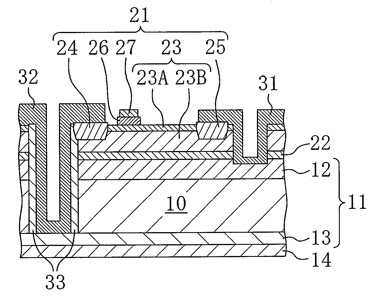
[0032]Hereinafter, a first embodiment of the present invention will be described with reference to the figures. FIG. 1 shows a cross-sectional structure of a semiconductor device according to the first embodiment. As shown in FIG. 1, the semiconductor device of the first embodiment includes a semiconductor substrate 10 and a hetero-junction transistor (HFET) 21. The semiconductor substrate 10 is an n-type silicon substrate having a diode 11 formed therein. The HFET 21 is made of a nitride semiconductor and is formed over the semiconductor substrate 10.

[0033]The diode 11 is a PIN (p-intrinsic-n) diode and has a cathode 12 formed on a first surface side of the semiconductor substrate 10 and an anode 13 formed on a second surface side of the semiconductor substrate 10. The cathode 12 is an n-type region made of an n-type impurity diffusion layer. The anode 13 is a p-type region made of a p-type impurity diffusion layer and is ohmic-connected to a back electrode 14 formed on the second ...

first modification

of First Embodiment

[0046]Hereinafter, a first modification of the first embodiment will be described with reference to the figures. FIG. 6 shows a cross-sectional structure of a semiconductor device according to the first modification of the first embodiment. In FIG. 6, the same elements as those of FIG. 1 are denoted by the same reference numerals and characters, and description thereof will be omitted.

[0047]The semiconductor device of the first modification has a diffusion prevention layer 17 formed between a cathode 12 that is an n-type region and a semiconductor layer laminate 23. The diffusion prevention layer 17 is made of silicon oxide (SiO2) or the like and prevents diffusion of a group-III element contained in a nitride semiconductor. Ga or the like that is a group-III element functions as p-type impurities to silicon. Therefore, if Ga diffuses into the cathode 12 that is an n-type region, the cathode 12 may turn into a p-type region, degrading diode characteristics. Formin...

second modification

of First Embodiment

[0060]Hereinafter, a second modification of the first embodiment will be described with reference to the figures. FIG. 9 shows a cross-sectional structure of a semiconductor device according to the second modification of the first embodiment. In FIG. 9, the same elements as those of FIG. 1 are denoted by the same reference numerals and characters, and description thereof will be omitted. As shown in FIG. 9, in the semiconductor device of the second modification, a second surface of a semiconductor substrate 10 is an element formation surface and an HFET 21 is formed on the second surface. In this case, since a p-type region is formed on the HFET side, Ga diffusion from a nitride semiconductor layer into the semiconductor substrate would not cause any problems.

[0061]A Schottky barrier diode may be formed instead of a PIN diode. In this case, a source via plug 32 can be formed so as to form a Schottky junction with the semiconductor substrate 10 and can be used as a...


PUM


Abstract

A semiconductor device includes: a semiconductor substrate; a diode having a cathode formed on a first surface side of the semiconductor substrate and an anode formed on a second surface side of the semiconductor substrate; and a transistor formed over the semiconductor substrate. The transistor includes a semiconductor layer laminate formed over the semiconductor substrate, a source electrode and a drain electrode that are formed spaced apart from each other over the semiconductor layer laminate, and a gate electrode formed between the source electrode and the drain electrode. The source electrode is electrically connected to the anode, and the drain electrode is electrically connected to the cathode.

Description

CROSS-REFERENCE TO RELATED APPLICATIONS[0001]This application claims priority under 35 U.S.C. §119(a) on Japanese Patent Application No. 2007-339141 filed on Dec. 28, 2007, the entire contents of which are hereby incorporated by reference.BACKGROUND OF THE INVENTION[0002]1. Field of the Invention[0003]The present invention relates to a semiconductor device and a manufacturing method thereof. More particularly, the present invention relates to a nitride semiconductor device for use in a power supply circuit or the like, and a manufacturing method thereof.[0004]2. Related Art[0005]Nitride semiconductors such as gallium nitride (GaN), aluminum nitride (AlN), and indium nitride (InN) are wide-gap semiconductors having a wide bandgap. For example, GaN and AlN have a bandgap of 3.4 eV and 6.2 eV at room temperature, respectively. Nitride semiconductors are characterized by their higher breakdown field and higher saturated electron drift velocity than those of other compound semiconductors...

Claims


Application Information

Patent Timeline
Patent Type & Authority Applications(United States)
IPC IPC(8): H01L21/338H01L29/812
CPCH01L21/26533H01L21/743H01L21/76251H01L21/8252H01L27/0605H01L27/0629H01L29/872H01L29/2003H01L29/41766H01L29/7781H01L29/7783H01L29/861H01L29/1066H01L29/4175H01L21/8258
Inventor SHIBATA, DAISUKEMORITA, TATSUOYANAGIHARA, MANABUUEMOTO, YASUHIRO
Owner PANASONIC CORP
Why Eureka
Try Eureka