

Method for manufacturing integrated circuit and semiconductor structure of integrated circuit
a manufacturing method and semiconductor technology, applied in semiconductor devices, semiconductor/solid-state device details, electrical apparatus, etc., can solve the problems of increasing design complexity and chip area, poor uniformity of image, and increasing the output voltage value of rectangular shapes (e.g., driving circuits of displayers). , to achieve the effect of uniform doping concentration and stable output voltag
- Summary
- Abstract
- Description
- Claims
- Application Information
AI Technical Summary
Benefits of technology
Problems solved by technology
Method used
Image

Examples
first embodiment
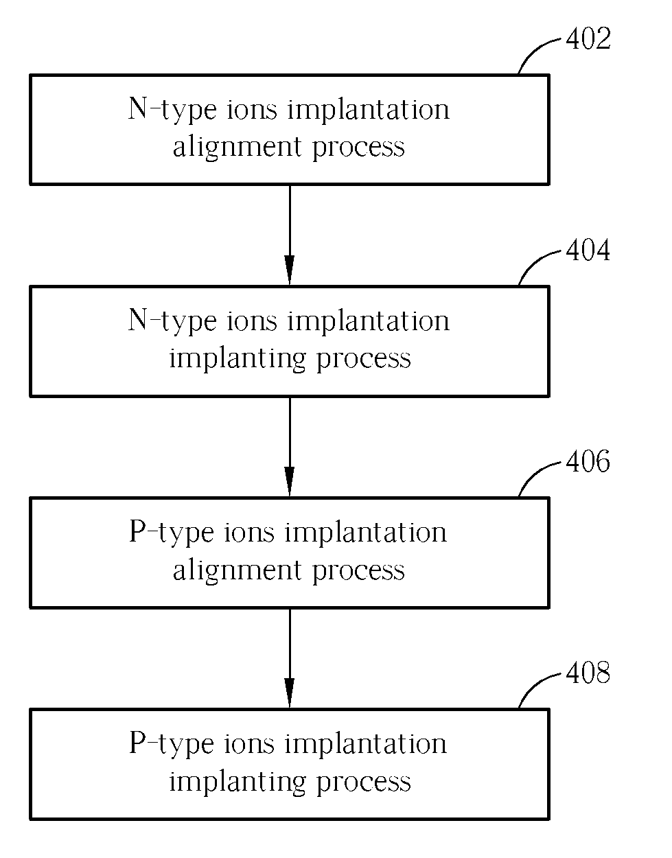
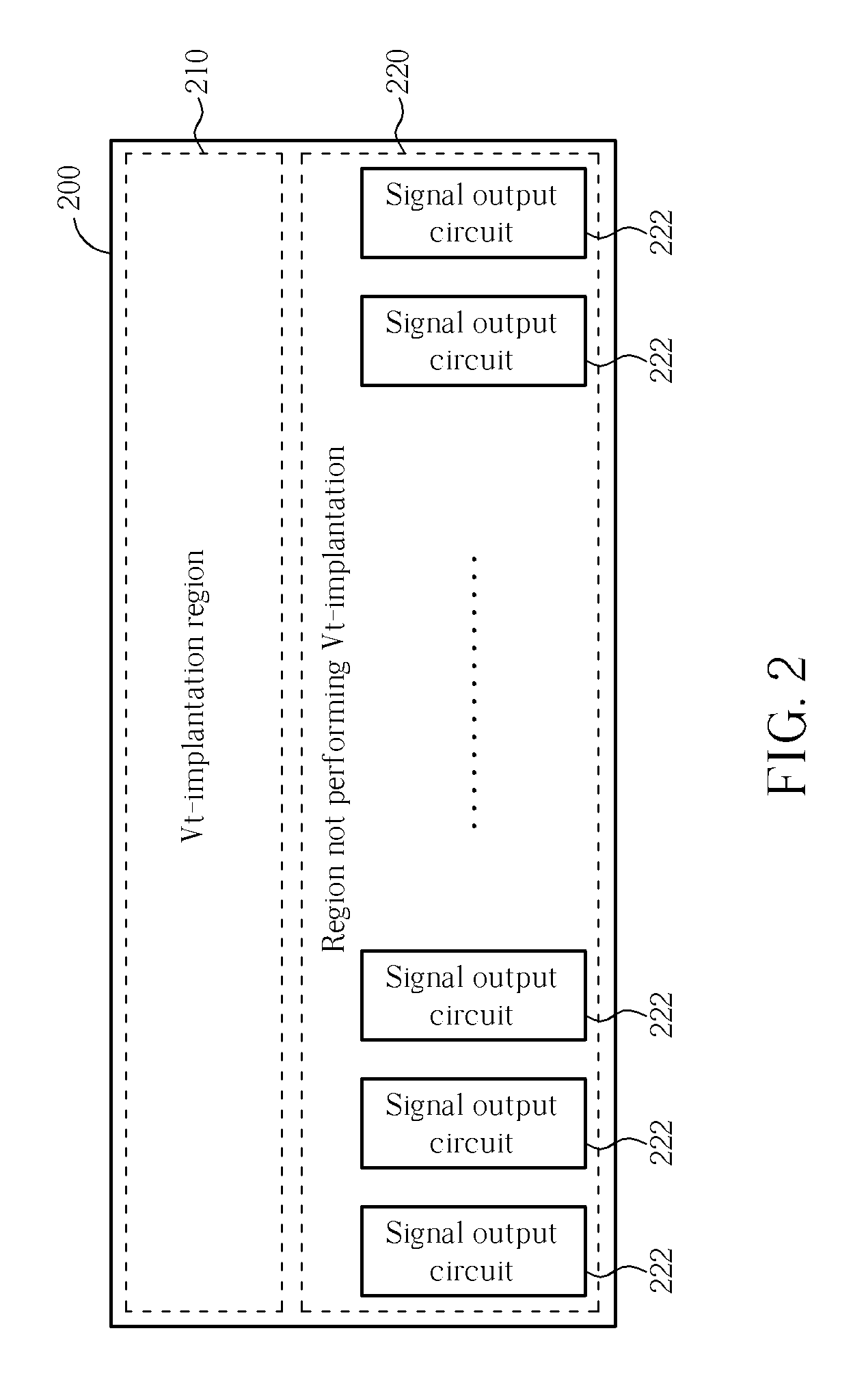
[0029]Additionally, in the above-mentioned embodiments of the present invention, all the transistors of the signal output circuits 222 in the chip 200 utilize the original doping concentration as the doping concentrations of the N-wells or the P-wells. However, considering functions of the signal output circuits 222, it is possible for N-wells or P-wells of only part of the transistors in the signal output circuits 222 to have the original doping concentration. Please refer to FIG. 5. FIG. 5 is a circuit diagram of the signal output circuit shown in FIG. 2 according to the present invention. As shown in FIG. 5, a circuit 500 comprises two regions 510 and 520 not having threshold voltage implantation performed thereon, a PMOS P3, an NMOS N3, and two current sources I1 and I2, where the region 510 comprises two PMOS P1 and P2, and the region 520 comprises two NMOS N1 and N2. In this embodiment, when performing threshold voltage implantation, the mask in Step 402 masks the NMOS N1 and ...
second embodiment
[0030]Please refer to FIG. 6. FIG. 6 is a circuit diagram of the signal output circuit shown in FIG. 2 according to the present invention. As shown in FIG. 6, a circuit 600 comprises two regions 610 and 620 not having threshold voltage implantation performed thereon, a NAND gate 612, a NOR gate 622, an inverter 630, four resistors R1, R2, R3, and R4, and a loading capacitor CL, where the region 610 comprises three PMOS P1, P2 and P3, and the region 620 comprises three NMOS N1, N2, and N3. When performing threshold voltage implantation, the mask in Step 402 masks the NMOS N1, N2, and N3 to make their N-wells have the original doping concentration nN—original after the N-type ions implantation implanting process in Step 404. Then, the mask in Step 406 masks the PMOS P1, P2, and P3 to make their P-wells have the original doping concentration nP—original after the P-type ions implantation implanting process in Step 408. It should be noted that, because the NAND gate 612, the NOR gate 62...
PUM
 Abstract
Description
Claims
Application Information