Quartz crystal resonator element, quartz crystal device, and method for producing quartz crystal resonator element
a resonator element and quartz crystal technology, applied in the direction of device details, device material selection, device details, etc., can solve the problems of insufficient energy trap, inability to extract stable signal from quartz crystal, and inability to secure space for providing thin sections, etc., to achieve high mass productivity, increase space occupied, and high mass productivity
- Summary
- Abstract
- Description
- Claims
- Application Information
AI Technical Summary
Benefits of technology
Problems solved by technology
Method used
Image
Examples
first embodiment
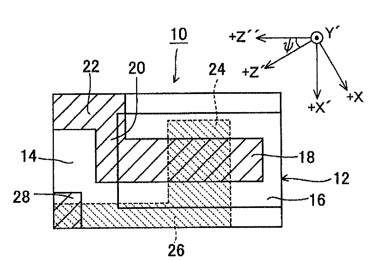
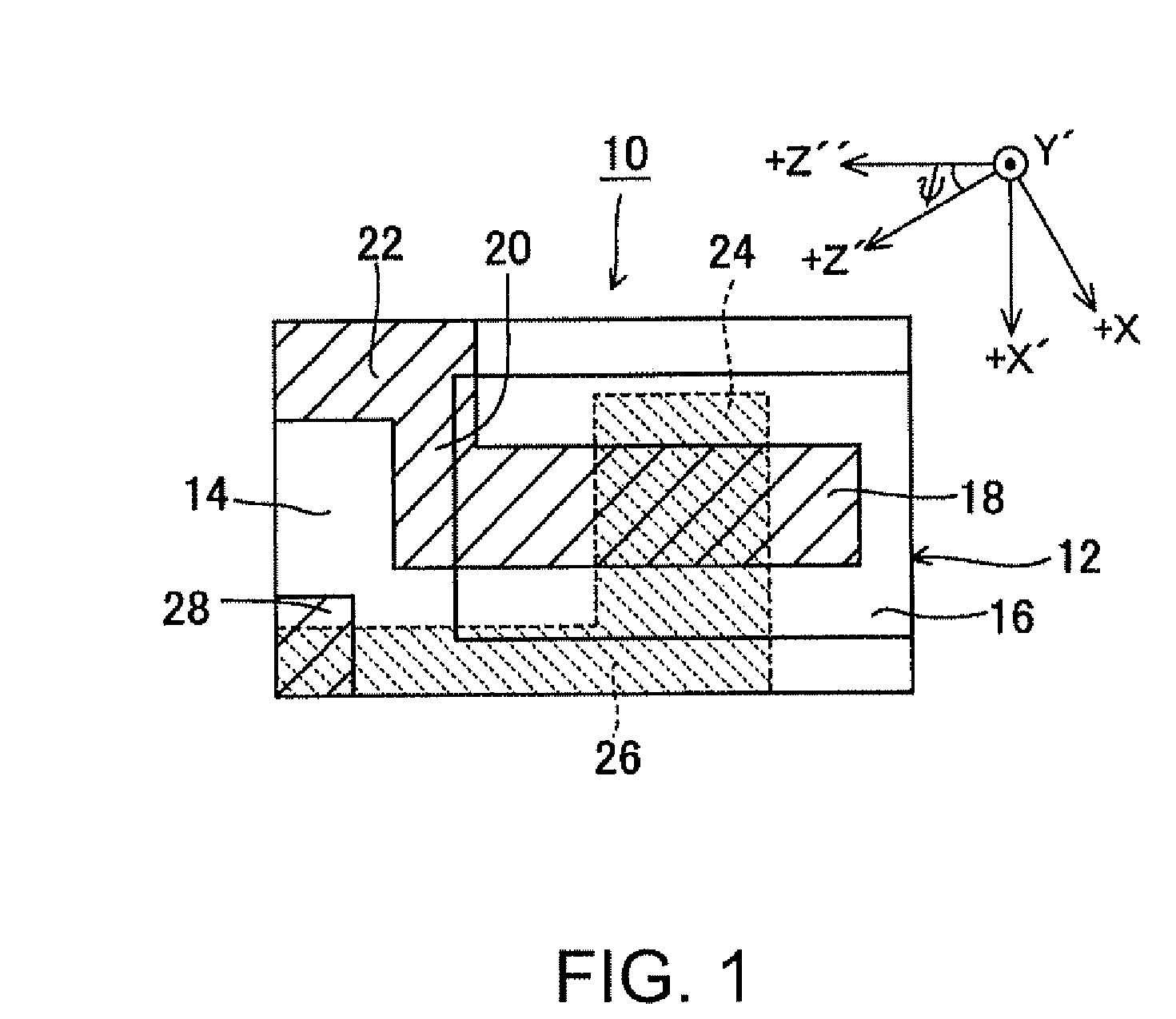
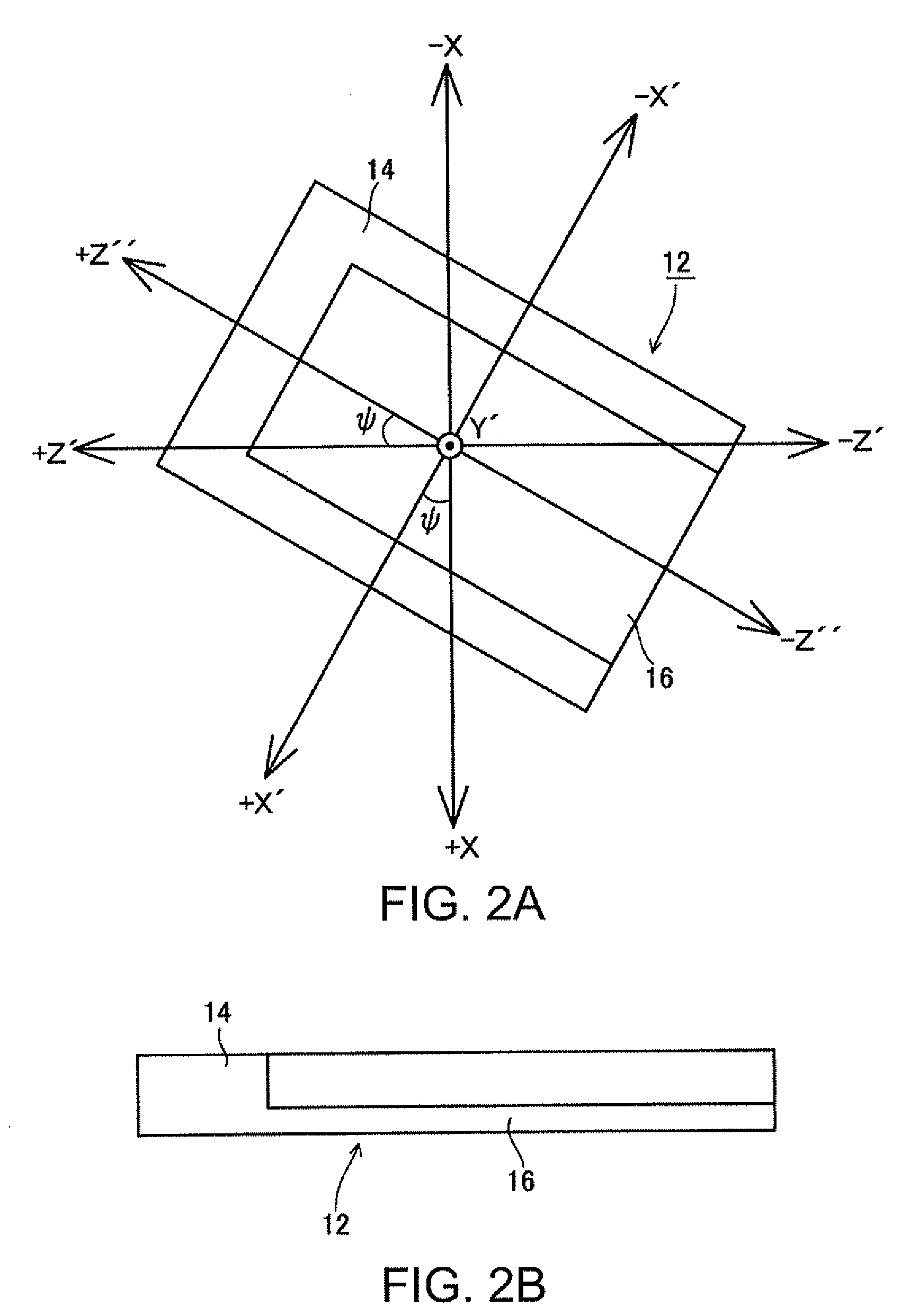
[0079]A quartz crystal resonator element 10 includes a quartz crystal substrate 12 and an electrode pattern formed on the quartz crystal substrate 12. In the quartz crystal resonator element 10 the quartz crystal substrate 12 is a so-called in-plane rotated AT-cut quartz crystal substrate. The AT-cut quartz crystal substrate is cut out in such a manner that a plane including an X axis and a Z axis as crystallographic axes of quartz crystal (a Y plane) is a main surface obtained by rotating a +Z axis by approximately 35° 15′ in a −Y-axis direction about the X axis as a reference point, namely a main surface including the X axis and a Z′ axis. Additionally, on the main surface including the X axis and the Z′ axis, when rotating a +Z′ axis in a +X-axis direction about a Y′ axis as a reference point is defined as having a positive rotation angle, the quartz crystal substrate 12 used in the embodiment has edges along (parallel to) an X′ axis and an Z″ axis obtained by rotating each of t...
second embodiment
[0111]Next, the mask 32 is once removed, and then, the second etching process is performed. The second etching process forms the mask 32 to cover a region except for the penetrating-groove-forming regions including the outer peripheral portions of the thick-section-forming regions and the outer peripheral portions of the non-thick-section-forming regions, namely to cover the individual-element-forming region 36 included in each quartz crystal substrate 12 and the break-off portion 40. In addition, in the second embodiment, the masks 32 and 44 (See FIGS. 21A to 21C), respectively, are formed on the upper and the lower surfaces, respectively. The mask 44 on the lower surface is, as in the mask 32 on the upper surface, formed to cover portions except for the penetrating-groove-forming regions.
[0112]Wet etching is performed on both of the upper and the lower surfaces of the wafer 30 having the masks 32 and 44 formed as above. The etching for forming the penetrating groove 38a is simulta...
third embodiment
[0130]As described above, on the AT-cut quartz crystal substrate, changing the in-plane rotation angle causes a difference concerning residues generated at the stepped portion between the thin resonating section and the thick section. Setting the rotation angle in the above range can increase the probability of generation of the residues on the +X′-axis side and the −Z″-axis side of the resonating section. Accordingly, in the quartz crystal resonator element 10b the thick section that forms the edges of the −X′-axis side and the −Z″-axis side is set as an etching range, thereby increasing a space occupied by the thin section as a resonating section 16b.
[0131]An electrode pattern arranged on the quartz crystal resonator element 10b according to the third embodiment thus structured is almost the same as the electrode pattern of the quartz crystal resonator element 10a according to the second embodiment, excepting that there is a difference associated with a change in the arranging p...
PUM
| Property | Measurement | Unit |
|---|---|---|
| rotation angle | aaaaa | aaaaa |
| rotation angle | aaaaa | aaaaa |
| in-plane rotation angle | aaaaa | aaaaa |
Abstract
Description
Claims
Application Information


