Multi-chip package

Active Publication Date: 2009-07-09
SEMICON COMPONENTS IND LLC
View PDF70 Cites 24 Cited by
  • Summary
  • Abstract
  • Description
  • Claims
  • Application Information

AI Technical Summary

Benefits of technology

[0019]The present invention provides a multi-chip package having an insulation structure with

Problems solved by technology

Also, power devices also desirably have low heat generation, high heat dissipation, and high reliability.
The EMC limits the ability of the power circuit chip to release heat to the outside of the power semiconductor module package.
Secondly, the fabrication process of the power semiconductor module package is complicated because two EMCs having different properties are used for one power semiconductor module package.
Thirdly, if a plurality of semiconductor chips is mounted on the lead frame, it is not

Method used


Image

  • Multi-chip package
  • Multi-chip package
  • Multi-chip package

Examples


Embodiment Construction

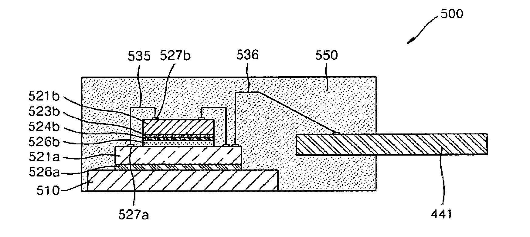
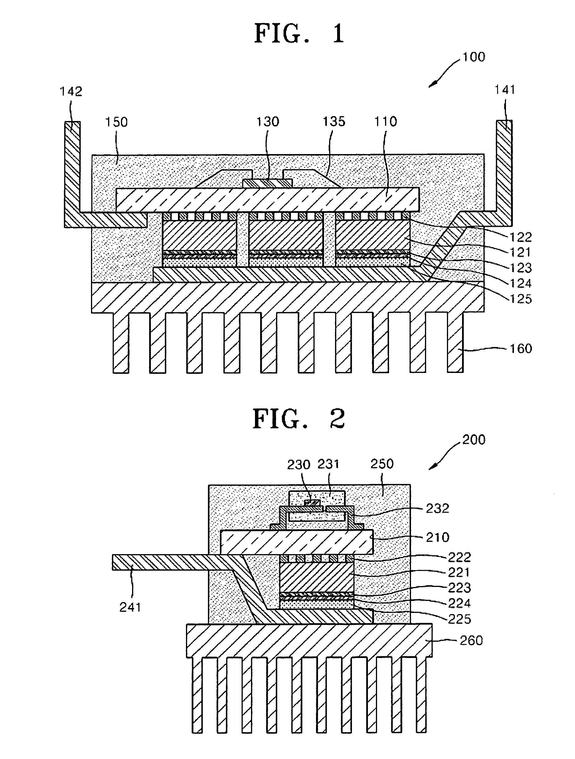
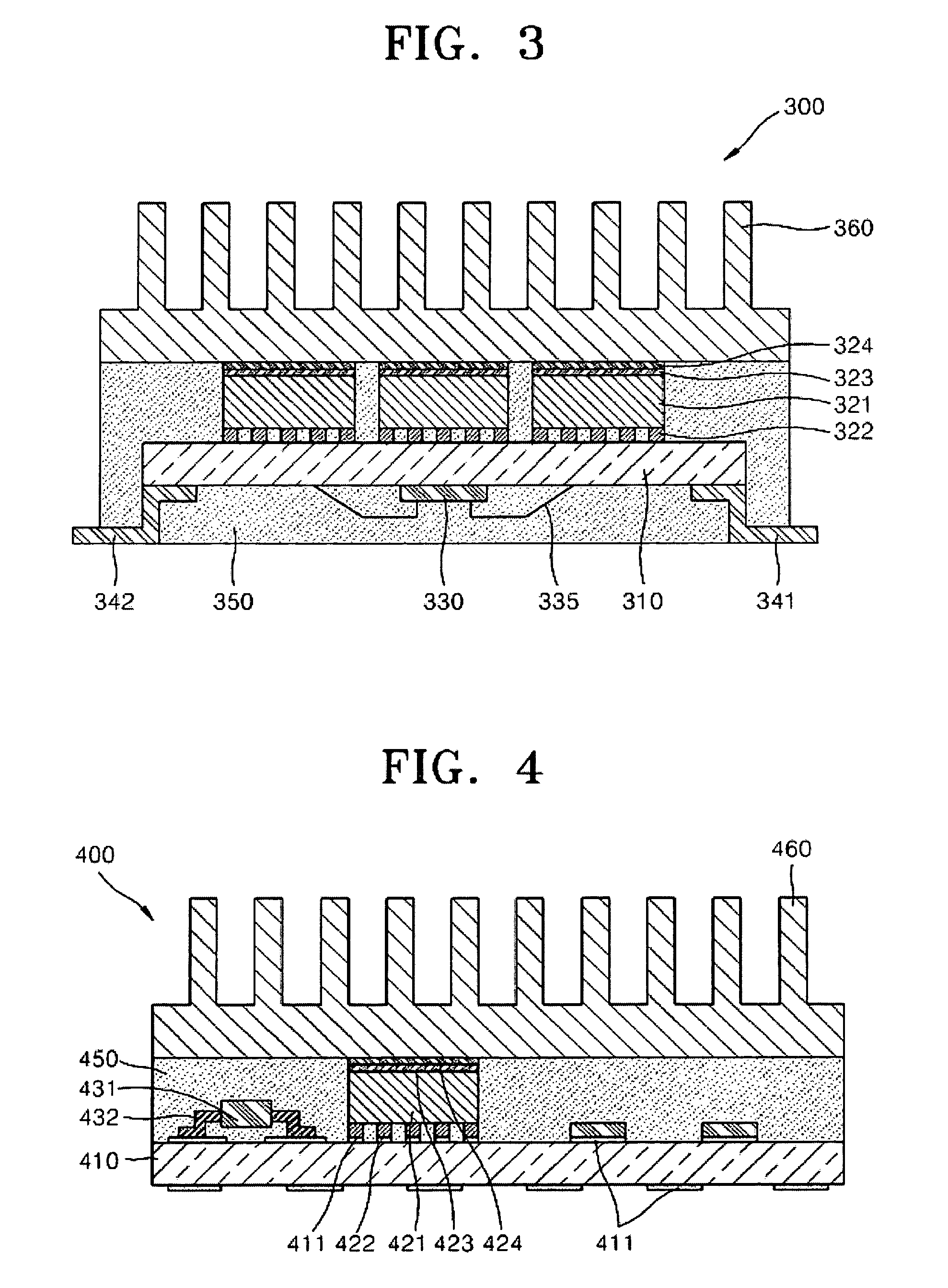
[0031]Reference will now be made in detail to a number of exemplary embodiments, which are shown in the accompanying drawings. However, embodiments of the invention are not limited to the exemplary embodiments described herein, and other embodiments may be within the scope and spirit of the invention. In the drawings, the thicknesses of layers and regions may be exaggerated for clarity of illustration.

[0032]Like reference numerals refer to like elements throughout. It will be understood that when an element, such as a layer, a region, or a substrate, is referred to as being “on,” another element, it may be directly on the other element or intervening elements may be present. Spatially relative terms, such as “above,”“upper,”“beneath,”“below,”“lower,” and the like, may be used herein for ease of description to describe one element or feature's relationship to another element(s) or feature(s) as illustrated in the figures. It will be understood that the spatially relative terms are in...


PUM


Abstract

A semiconductor package is disclosed. Particularly, a multi-chip package is disclosed, which can stably maintain insulation between a plurality of semiconductor chips and effectively release heat to the outside. The semiconductor package includes an insulation layer including a diamond layer formed by a chemical vapor deposition method between a lead frame or a heat sink and the semiconductor chips disposed thereon.

Description

CROSS-REFERENCES TO RELATED APPLICATIONS[0001]This application claims the benefit of Korean Patent Application No. 10-2007-0129964, filed on Dec. 13, 2007, in the Korean Intellectual Property Office, the disclosure of which is incorporated herein in its entirety by reference.STATEMENT AS TO RIGHTS TO INVENTIONS MADE UNDER FEDERALLY SPONSORED RESEARCH OR DEVELOPMENT[0002]NOT APPLICABLEREFERENCE TO A “SEQUENCE LISTING,” A TABLE, OR A COMPUTER PROGRAM LISTING APPENDIX SUBMITTED ON A COMPACT DISK[0003]NOT APPLICABLEBACKGROUND OF THE INVENTION[0004]1. Field of the Invention[0005]The present invention relates to a semiconductor package, and more particularly, to a multi-chip package including one or more semiconductor chips.[0006]2. Description of the Related Art[0007]In a general semiconductor package, one or a plurality of semiconductor chips are encapsulated with an epoxy mold compound (EMC) for protection, and are mounted on a printed circuit board (PCB).[0008]It is desirable for elec...

Claims


Application Information

Patent Timeline
IPC IPC(8): H01L23/34H01L23/52H01L21/56H01L21/98
CPCH01L21/56H01L2924/10253H01L23/433H01L23/4334H01L23/49531H01L23/49575H01L24/31H01L25/16H01L2224/16225H01L2224/48227H01L2224/48247H01L2224/73253H01L2224/73265H01L2924/01013H01L2924/01029H01L2924/01047H01L2924/01074H01L2924/01082H01L24/48H01L2924/01006H01L2924/01033H01L2224/32245H01L23/3107H01L2924/00H01L2924/15747H01L2924/181H01L2924/00014H01L2924/00012H01L2224/45099H01L2224/45015H01L2924/207H01L23/12H01L23/28
Inventor EOM, JOO-YANGPARK, MIN-HYOCHOI, SEUNG-YONG
Owner SEMICON COMPONENTS IND LLC
Why Eureka
Try Eureka