Power amplifier

a power amplifier and amplifier technology, applied in the direction of amplifiers with semiconductor devices only, amplifiers with semiconductor devices, amplifiers with control details, etc., can solve the problems of large impedance mismatches, inability to perform design of power amplifiers and bypass circuits independently of each other, and difficulty in matching impedance in amplification mode and attenuation mode, so as to reduce the minimum operating voltage, reduce input and output impedance mismatches, and increase the degree of design freedom

Active Publication Date: 2009-07-09
MURATA MFG CO LTD
View PDF9 Cites 14 Cited by
  • Summary
  • Abstract
  • Description
  • Claims
  • Application Information

AI Technical Summary

Benefits of technology

[0021]The circuit shown in FIGS. 24 and 25 has problems described below. First, a large impedance mismatch can occur easily between the first and second stages and between the second and third stages when the second-stage power amplifier A2 is turned off. This is because each of the matching circuits between the first and second stages and between the second and third stages is configured only of passive elements, and because this configuration makes impedance matching both in the amplification mode and in the attenuation mode difficult. If an impedance mismatch between the stages is large, it easily becomes a cause of oscillation of the amplifier when the load changes and generation of a reflection gain, which is undesirable to the operation.
[0023]In view of the above-described problems, an object of the present invention is to provide a power amplifier capable of reducing the minimum operating voltage, reducing input and output impedance mismatches in an attenuation mode and increasing the degree of design freedom.
[0025]The present invention reduces the minimum operating voltage, reduces input and output impedance mismatches in the attenuation mode and increases the degree of design freedom.

Problems solved by technology

Also, there is a problem that if a drive circuit for the attenuator is also formed by GaAs-HBTs, the minimum operating voltage is theoretically 3 Vbi or higher (about 3.6 to 3.9 V) because of a need to supply voltages to the control terminals Vc1 and Vc4 through the emitters of the HBTs.
First, a large impedance mismatch can occur easily between the first and second stages and between the second and third stages when the second-stage power amplifier A2 is turned off.
This is because each of the matching circuits between the first and second stages and between the second and third stages is configured only of passive elements, and because this configuration makes impedance matching both in the amplification mode and in the attenuation mode difficult.
If an impedance mismatch between the stages is large, it easily becomes a cause of oscillation of the amplifier when the load changes and generation of a reflection gain, which is undesirable to the operation.
Also, since the resistance Rf2 and the capacitor Cf2 operate as a feedback circuit in the amplification mode, design of the power amplifier and design of the bypass circuit cannot be performed independently of each other.
That is, factors including the transistor size of the power amplifier and the amount of attenuation by the bypass circuit cannot be freely designed.

Method used


Image

  • Power amplifier
  • Power amplifier
  • Power amplifier

Examples


first embodiment

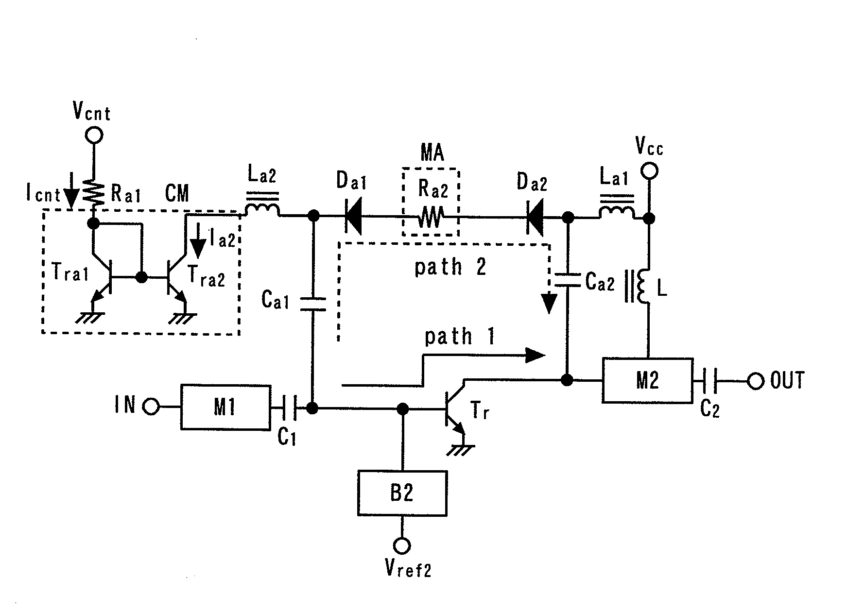
[0052]FIG. 1 is a circuit diagram showing a power amplifier according to a first embodiment of the present invention. This power amplifier is formed by a GaAs-HBT process.

[0053]An amplifying transistor Tr which amplifies an RF signal has its base connected to an input terminal IN via an input matching circuit M1 and a capacitor C1 (first capacitor), has its collector connected to an output terminal OUT via an output matching circuit M2 and a capacitor C2 and has its emitter grounded. An inductor L is provided between a collector power supply terminal Vcc and the output matching circuit M2. A bias circuit B2 supplies a bias current to the base of the amplifying transistor Tr according to a voltage applied to a control terminal Vref.

[0054]The cathode of a BC diode Da1 (first diode) is connected to the input terminal IN via a capacitor Ca1 (second capacitor), the capacitor C1 and the input matching circuit M1. The anode of a BC diode Da2 (second diode) is connected to the output termin...

second embodiment

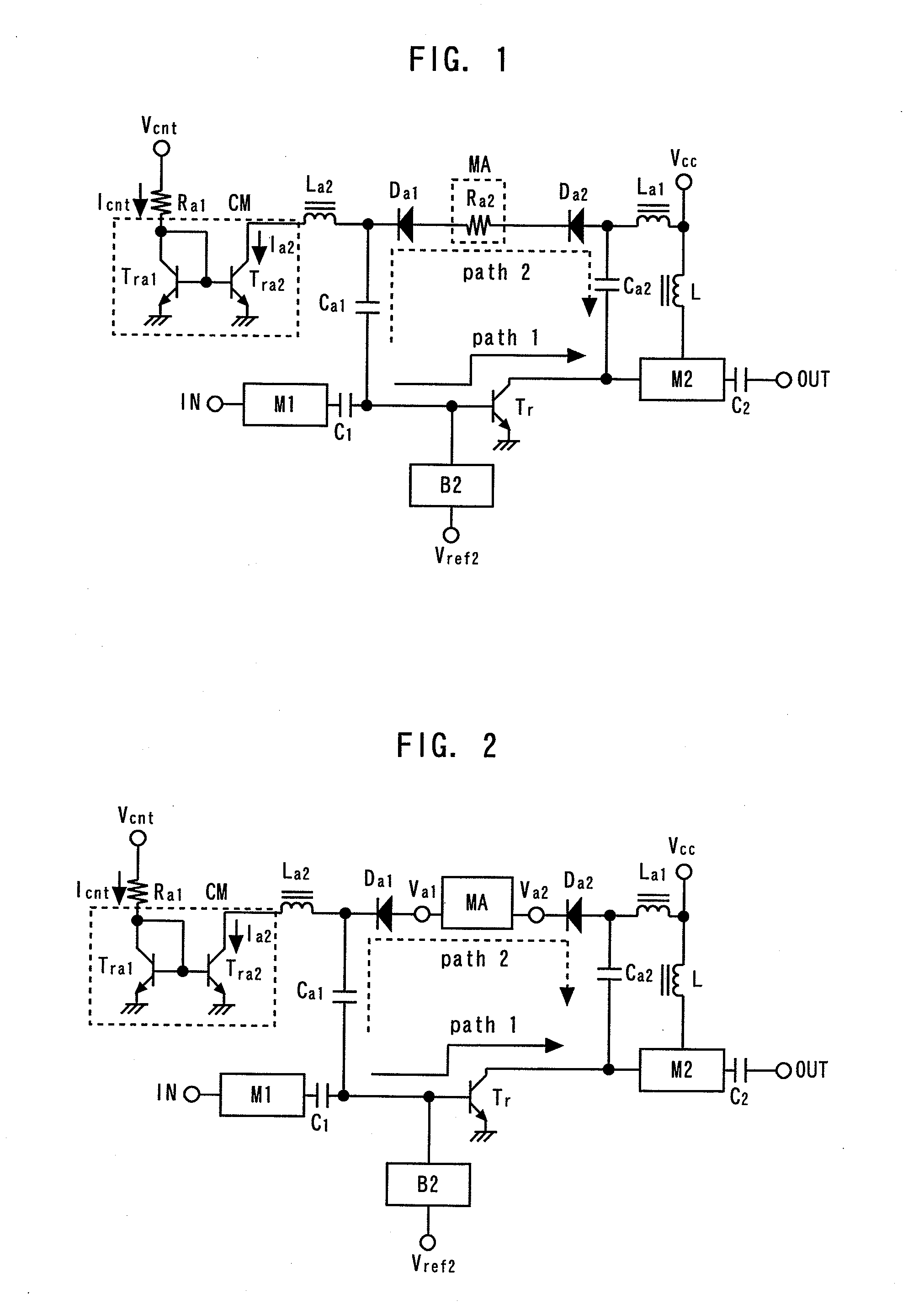
[0062]FIG. 2 is a circuit diagram showing a power amplifier according to a second embodiment of the present invention. The second embodiment differs from the first embodiment in the configuration of the matching and attenuating circuit MA. The circuit configuration of the matching and attenuating circuit according to the second embodiment will be described. It is assumed here that the matching and attenuating circuit MA has a terminal Va1 connected to the anode of the BC diode Da1 and a terminal Va2 connected to the cathode of the BC diode Da2.

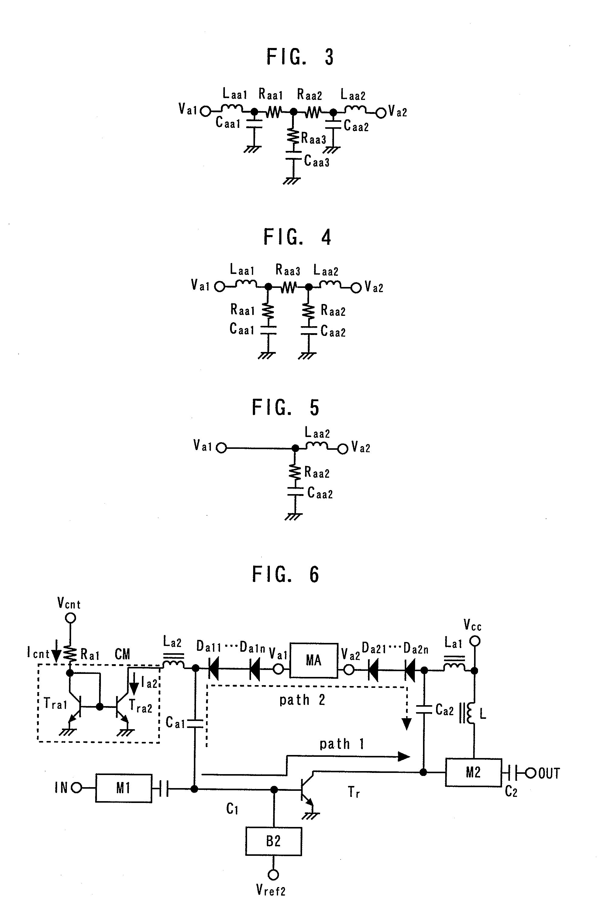
[0063]FIG. 3 is a circuit diagram showing a first example of the matching and attenuating circuit according to the second embodiment. An inductor Laa1, a resistor Raa1, a resistor Raa2 and an inductor Laa2 are connected in series between the terminal Va1 and the terminal Va2. A capacitor Caa1 is connected between an inductor Laa1-resistor Raa1 connection point and a grounding point. A resistor Raa3 and a capacitor Caa3 are connected in series ...

third embodiment

[0067]FIG. 6 is a circuit diagram showing a power amplifier according to a third embodiment of the present invention. The third embodiment differs from the second embodiment in that each of the first and second diodes comprises a plurality of diodes connected in series. That is, a plurality of BC diodes Da11 to Da1n are connected in series as the first diode in place of the BC diode Da1, and a plurality of BC diodes Da21 to Da2n are connected in series as the second diode in place of the BC diode Da2. In this way, insufficiency of isolation of the path 2 in the amplification mode can be remedied. Other effects, which are the same as those of the second embodiment, can also be obtained.


PUM


Abstract

An amplifying transistor for amplifying a radio frequency signal between an input terminal and an output terminal. The cathode of a first diode is connected to the input terminal and the anode of a second diode is connected to the output terminal. A matching and attenuating circuit is connected between the anode of the first diode and the cathode of the second diode. A matching and attenuating circuit reduces impedance mismatches on the input terminal side and the output terminal side, and attenuates the radio frequency signal. In an amplification mode, a bias circuit supplies a bias current to an amplifying transistor and a current mirror circuit turns off the first and second diodes. In an attenuation mode, the bias circuit supplies no bias current to the amplifying transistor and the current mirror circuit turns on the first and second diodes.

Description

BACKGROUND OF THE INVENTION[0001]1. Field of the Invention[0002]The present invention relates to a power amplifier which amplifies a radiofrequency (RF) signal in an amplification mode, and which attenuates an RF signal in an attenuation mode. More particularly, the present invention relates to a power amplifier capable of increasing the degree of design freedom by reducing the minimum operating voltage and reducing input and output impedance mismatches in the attenuation mode.[0003]2. Background Art[0004]In recent years, GaAs-HBT (heterojunction bipolar transistor) power amplifiers have been widely used as a power amplifier for portable telephones for code division multiple access (CDMA) and a power amplifier for wireless LANs.[0005]Because GaAs-HBTs do not require a negative gate bias voltage, they can operate by being powered from a single power supply and obtaining uniform device characteristics in comparison with GaAs-FETs. Therefore GaAs-HBTs have been frequently applied to Ga...

Claims


Application Information

Patent Timeline
Patent Type & Authority Applications(United States)
IPC IPC(8): H03G3/30
CPCH03G1/0052H03F3/191H03F3/213H03F3/12
Inventor YAMAMOTO, KAZUYAMIYASHITA, MIYO
Owner MURATA MFG CO LTD
Why Eureka
Try Eureka