High-K Dielectric Stack And Method Of Fabricating Same

a dielectric layer and high-k technology, applied in the field of high-k dielectric stacks, can solve the problems of degrading the electrical performance of the igi layer, not providing strong nitridization of the underlying gate insulating film, and a large number of structural defects, so as to improve the reliability of the high-k dielectric layer

Active Publication Date: 2009-07-16
TOWER SEMICONDUCTOR
View PDF5 Cites 41 Cited by
  • Summary
  • Abstract
  • Description
  • Claims
  • Application Information

AI Technical Summary

Benefits of technology

[0009]Accordingly, the present invention provides a method for improving the reliability of a high-k dielectric layer or a high-k dielectric stack by forming an amorphous high-k dielectric layer over a silicon oxide layer, doping the amorphous high-k dielectric layer w...

Problems solved by technology

However, the conductive properties of the gate electrode (i.e., polysilicon sheet resistance) will necessarily be degraded by the introduction of nitrogen into the gate electrode.
Moreover, a major portion of the introduced nitrogen remains in the gate electrode (polysilicon) during subsequent post doping bakes (due to a hig...

Method used


Image

  • High-K Dielectric Stack And Method Of Fabricating Same
  • High-K Dielectric Stack And Method Of Fabricating Same
  • High-K Dielectric Stack And Method Of Fabricating Same

Examples


Embodiment Construction

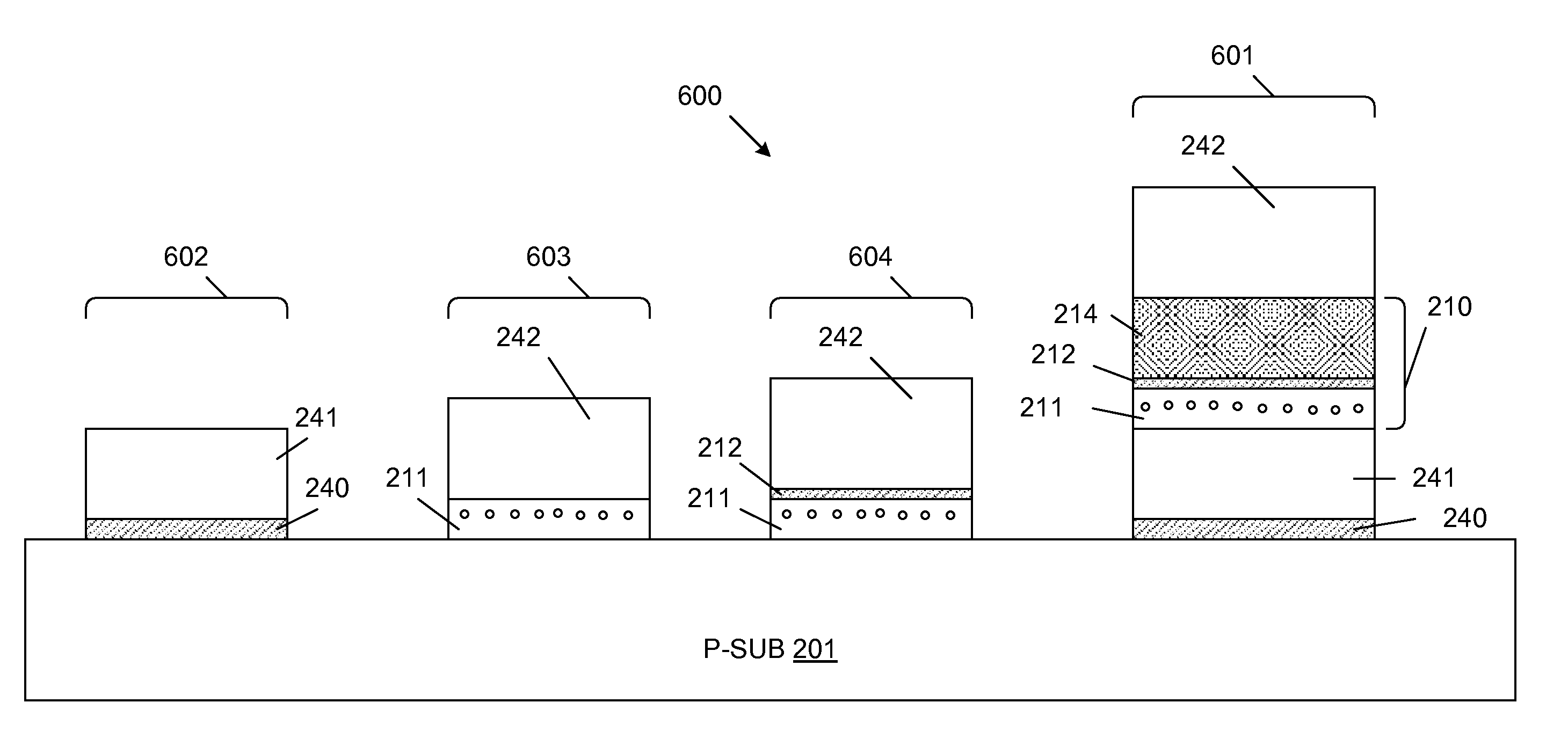
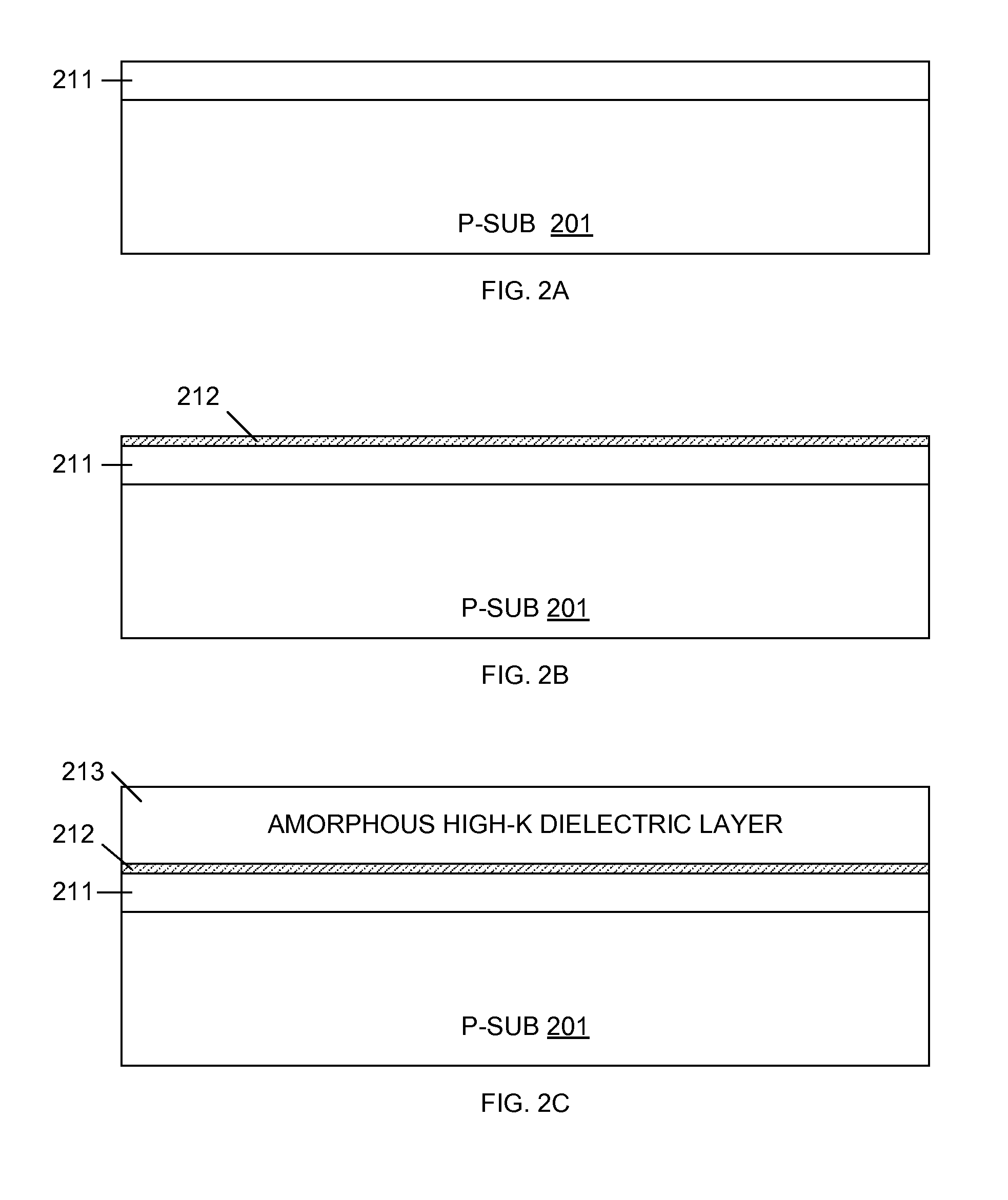
[0026]FIGS. 2A, 2B, 2C, 2D and 2E are cross sectional views of a high-k dielectric stack during various stages of fabrication, in accordance with one embodiment of the present invention.

[0027]As illustrated in FIG. 2A, an insulating layer 211 is formed over an upper surface of a semiconductor substrate 201. In the described embodiment, substrate 201 is p-type monocrystalline silicon. Semiconductor substrate 201 may have an n-type conductivity in other embodiments. Insulating layer 211 can be fabricated using the same growth conditions used to form the first layer of a conventional ONO structure or a CMOS transistor gate dielectric layer. For example, insulating layer 211 can be silicon oxide formed by dry thermal oxidation of the underlying silicon substrate 201. Insulating layer 211 can be formed in other manners in other embodiments. In accordance with one embodiment, the thickness of silicon oxide layer 211 is selected to correspond with a desired gate dielectric thickness of CMO...


PUM


Abstract

A method for improving the reliability of a high-k dielectric layer or a high-k dielectric stack by forming an amorphous high-k dielectric layer over an insulating layer, doping the amorphous high-k dielectric layer with nitrogen atoms, and subsequently heating the resulting structure at a temperature greater than or equal to the crystallization temperature of the high-k dielectric material, thereby transforming the high-k dielectric material from an amorphous state to a crystalline state, and causing nitrogen atoms to diffuse into the insulating layer.

Description

FIELD OF THE INVENTION[0001]The present invention relates to high-k dielectric stacks. More specifically, the present invention relates to high-k dielectric stacks having a nitrided crystalline high-k dielectric layer and a silicon oxide layer that is nitrided by outdiffusion from the nitrided crystalline high-k dielectric layer.RELATED ART[0002]In the past, nitrogen has been introduced during the fabrication of semiconductor devices in order to modify the characteristics of these semiconductor devices.[0003]For example, U.S. Pat. No. 6,521,527 to Kuroi et al. describes a semiconductor device that includes a gate electrode that is doped with nitrogen, by directly introducing the nitrogen into the top portion of the electrode by ion implantation. The nitrogen occupies holes which would have provided diffusion paths for impurities that are subsequently introduced to the gate electrode. Thus, the nitrogen inhibits the out-diffusion of the impurities from the gate electrode to an underl...

Claims


Application Information

Patent Timeline
IPC IPC(8): H01L21/283
CPCH01L21/02178H01L29/792H01L21/022H01L21/02238H01L21/02255H01L21/02304H01L21/02332H01L21/02356H01L21/28185H01L21/28202H01L21/28282H01L21/3145H01L21/31612H01L21/3162H01L21/31645H01L21/823857H01L29/513H01L29/517H01L29/518H01L21/02181H01L29/40117
Inventor LISIANSKY, MICHAELROIZIN, YAKOVHEIMAN, ALEXEYFENIGSTEIN, AMOS
Owner TOWER SEMICONDUCTOR
Why Eureka
Try Eureka