

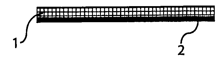
Method of forming a multilayer structure
a multi-layer structure and conductive electrode technology, applied in the direction of electrolysis components, vacuum evaporation coatings, coatings, etc., can solve the problems of large problem, reduced ecpr, and reduced ecpr, so as to reduce the risk of erosion or dishing or even eliminate the effect of ecpr
- Summary
- Abstract
- Description
- Claims
- Application Information
AI Technical Summary
Benefits of technology
Problems solved by technology
Method used
Image

Examples
Embodiment Construction
[0068]Below, embodiments including the best mode of the invention will be described in great detail in order to enable a skilled person to carry out the invention.
[0069]All embodiments described below comprise one or several of a number of method steps. Each of these steps will be described separately in detail below.
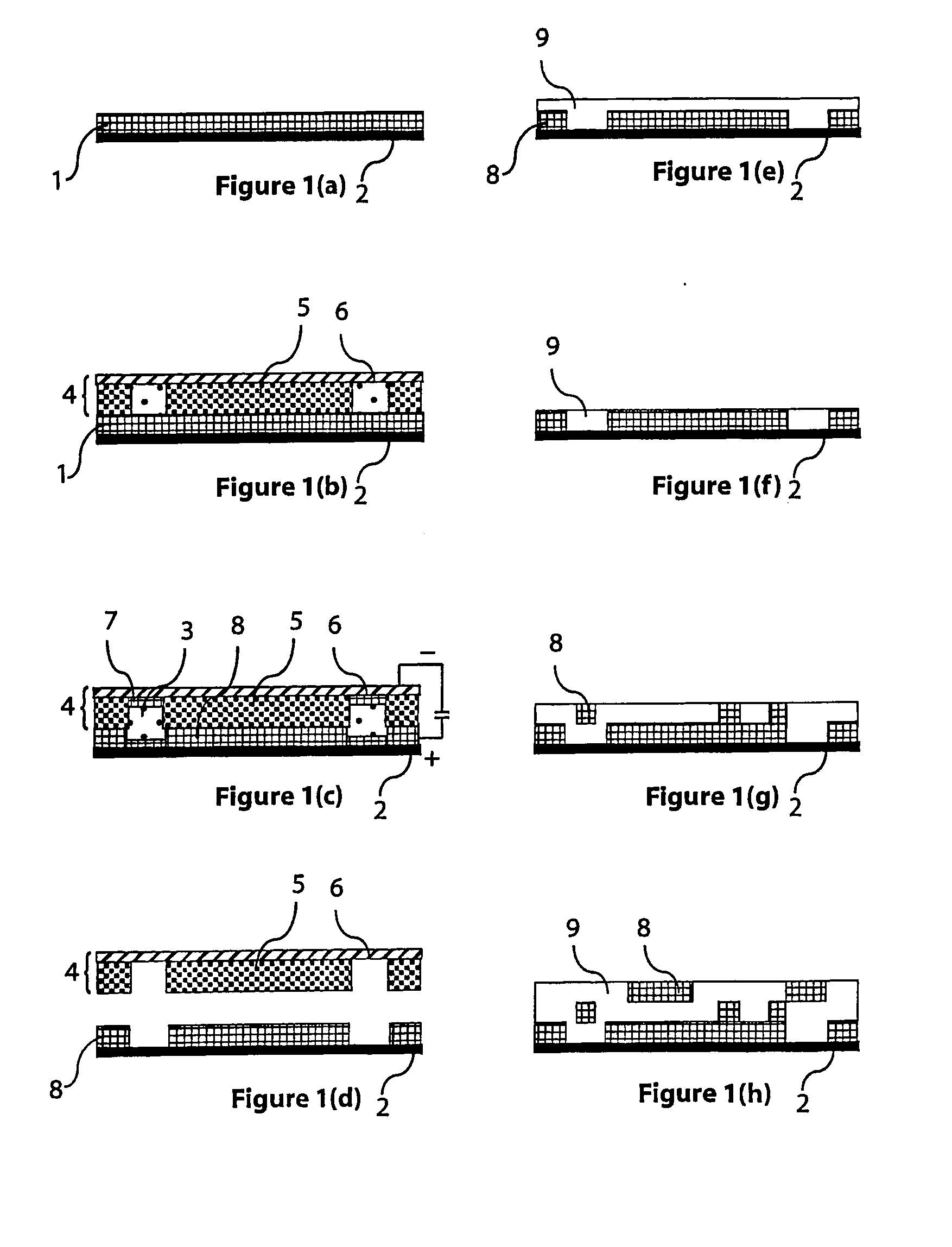
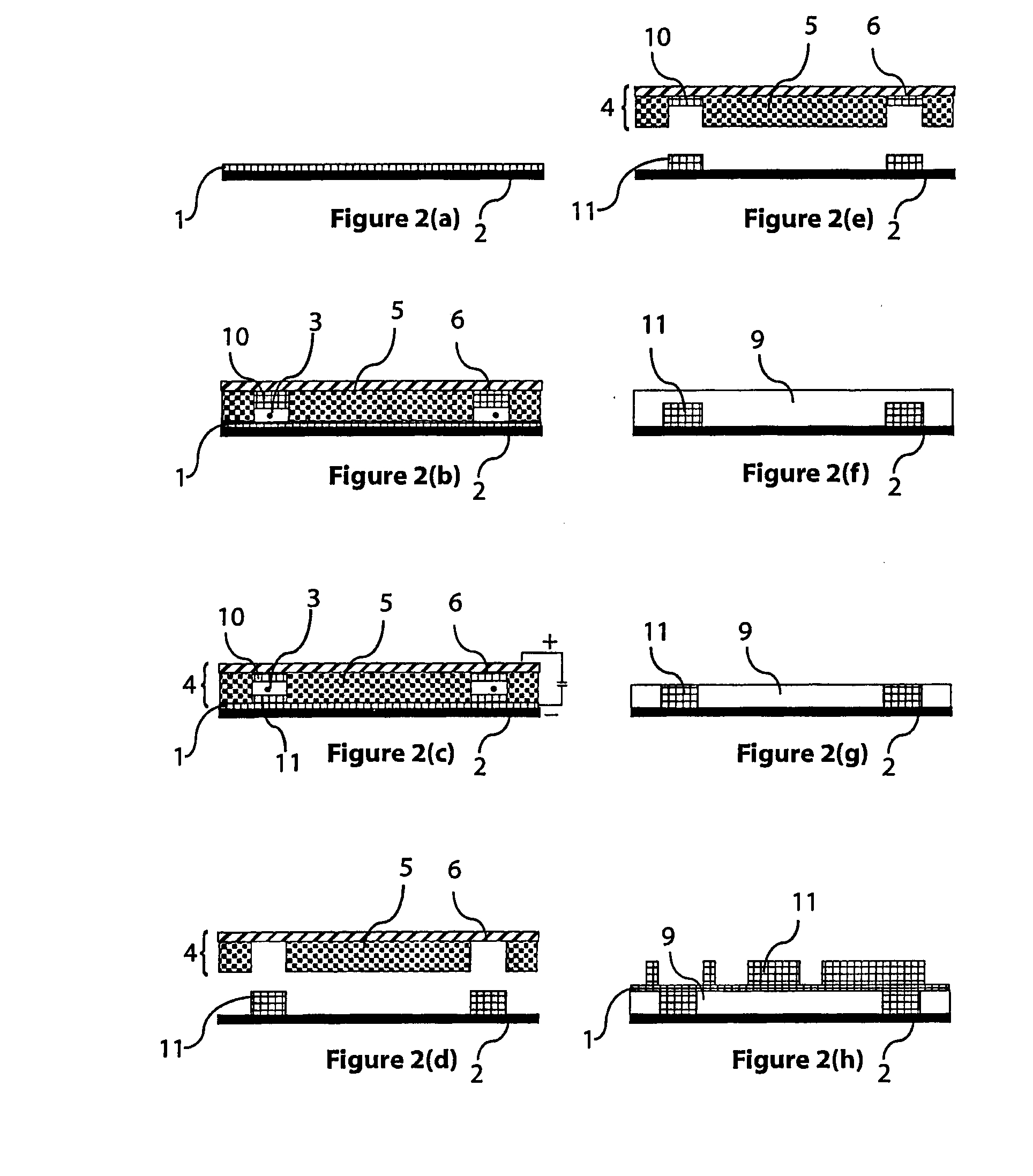
[0070]Generally, the method steps comprises one or several of the following six steps, namely:
[0071]a) arranging a seed layer on top of a substrate, or on top of a previous layer;
[0072]b) putting a master electrode in contact with the substrate, such as the seed layer, to form multiple electrochemical cells;
[0073]c) forming structures in said seed layer by etching or forming structures on said seed layer by plating;
[0074]d) removal of the master electrode;
[0075]e) possible removal of seed layer;
[0076]f) applying a dielectric material layer; and
possible planarizing and / or patterning of the dielectric material layer.
[0077]In a first step (a) the substrate is prepared by a...
PUM
| Property | Measurement | Unit |
|---|---|---|
| thickness | aaaaa | aaaaa |
| dielectric constants | aaaaa | aaaaa |
| electrically conducting | aaaaa | aaaaa |
Abstract
Description
Claims
Application Information