Semiconductor processing system including vaporizer and method for using same

a technology of semiconductors and processing systems, applied in the direction of casings/cabinets/drawers, loudspeakers, coatings, etc., can solve the problems of deterioration of vaporizing efficiency, nozzle clogging and/or spray abnormalities, and increase in residues, so as to achieve stably the effect of semiconductor processing

Inactive Publication Date: 2009-07-23
TOKYO ELECTRON LTD
View PDF2 Cites 201 Cited by
  • Summary
  • Abstract
  • Description
  • Claims
  • Application Information

AI Technical Summary

Benefits of technology

[0008]An object of the present invention is to provide a semiconductor processing system including a vaporizer for generating a process gas from a liquid material, and a method for using the system, which can prevent nozzle clogging of the vaporizer, thereby stably performing a semiconductor process, such as a film formation process, without stopping the semiconductor process.

Problems solved by technology

In this case, the solute of the liquid material is precipitated in the tip of the nozzle and causes nozzle clogging and / or spray abnormality.
Consequently, residues are increased due to a deterioration of the vaporizing efficiency, and case particle contamination on wafers.
Then, this substrate is discarded, because this substrate may be contaminated with particles of e.g., the organic metal precipitated due to a decrease in the pressure inside the vaporizing chamber.

Method used


Image

  • Semiconductor processing system including vaporizer and method for using same
  • Semiconductor processing system including vaporizer and method for using same
  • Semiconductor processing system including vaporizer and method for using same

Examples


first embodiment

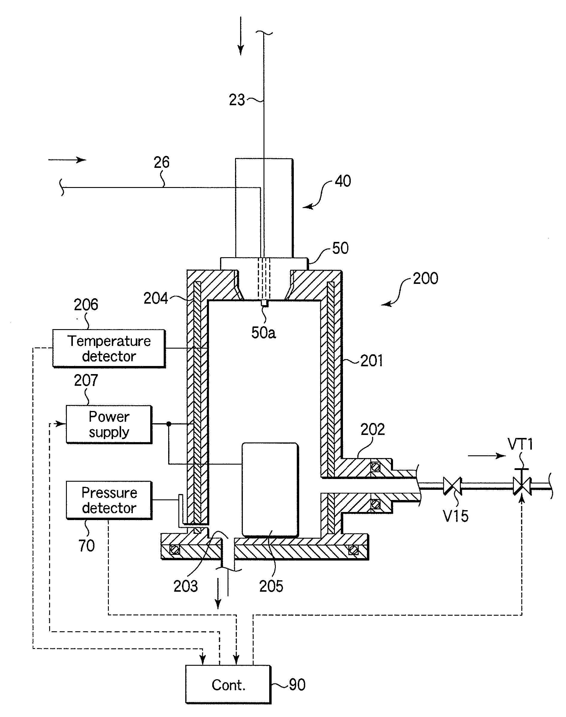
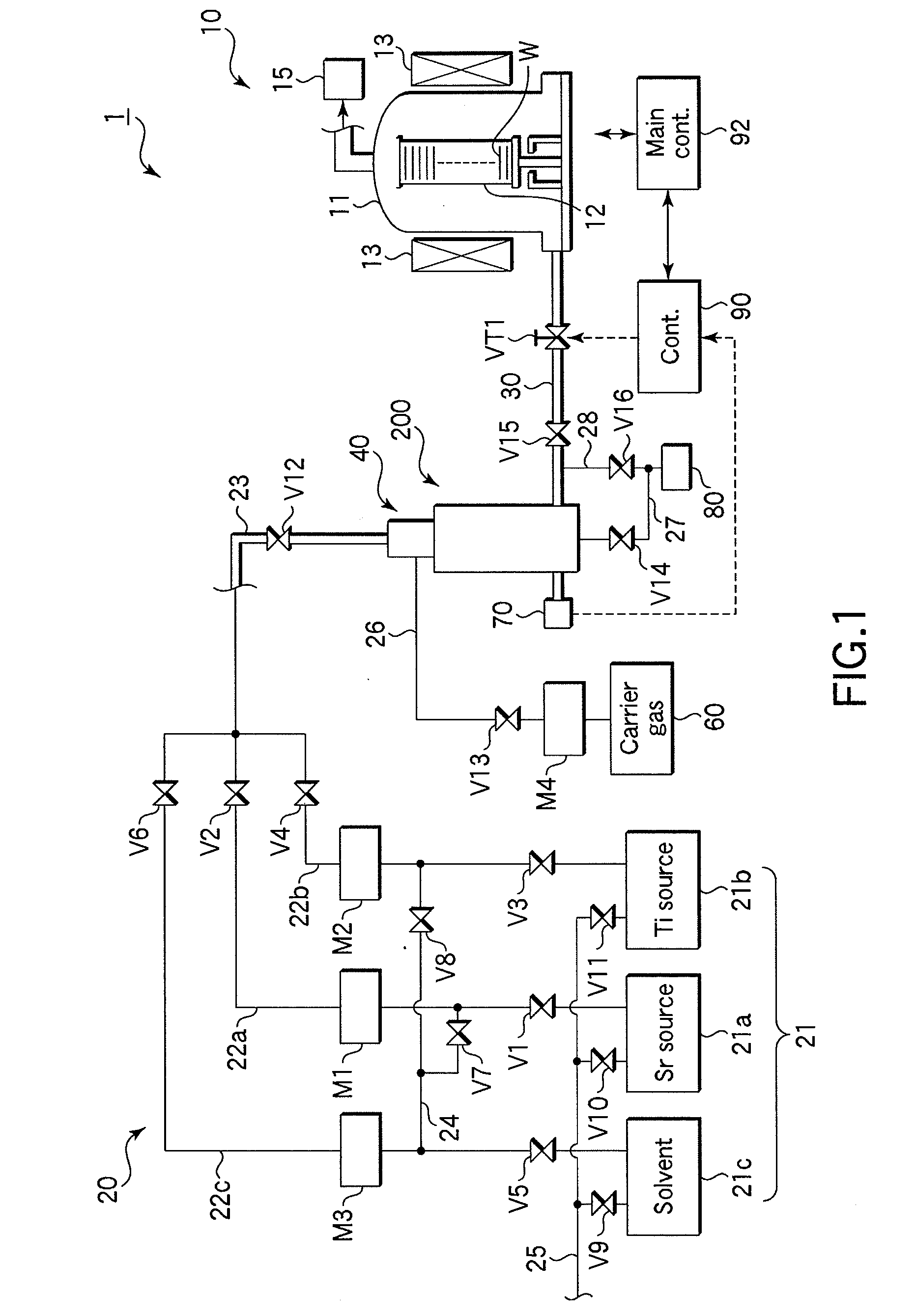
[0019]FIG. 1 is a structural view schematically showing a semiconductor processing system (film formation system) according to a first embodiment of the present invention. FIG. 2 is a sectional side view showing a vaporizer used in the gas supply apparatus of the system shown in FIG. 1. As shown in FIG. 1, the film formation system 1 according to this embodiment includes a film formation processing apparatus (semiconductor processing apparatus) 10 for performing a predetermined film formation process on target substrates, such as semiconductor wafers (which may be simply referred to as wafers), and a gas supply apparatus 20 for supplying a predetermined process gas into the film formation processing apparatus 10.

[0020]For example, the film formation section 10 comprises a low-pressure CVD apparatus of the batch type having a vertical reaction tube 11 used as a reaction chamber (process chamber). A wafer boat 12 that can support a number of wafers W is loaded and unloaded into and fr...

second embodiment

[0047]FIG. 4 is a structural view schematically showing a semiconductor processing system according to a second embodiment of the present invention. The film formation system 101 according to the second embodiment is arranged to control the pressure inside the vaporizing chamber by adjusting the flow rate of the solvent supplied to the liquid material supply line 23 by use of the flow rate regulator (serving as pressure adjusting means) M3 disposed on the solvent supply line 22c. Accordingly, this arrangement is an alternative to the arrangement of the first embodiment which controls the pressure by use of the regulator valve VT1 disposed on the process gas supply line 30. When the film formation system 101 is normally performs a process, it operates in the same way as the film formation system 1 according to the first embodiment.

[0048]Specifically, when a film formation process is started, the opening degree of the flow rate regulator M3 is set at zero so as not to supply the solve...

third embodiment

[0050]FIG. 5 is a structural view schematically showing a semiconductor processing system according to a third embodiment of the present invention. The film formation system 1001 according to the third embodiment is arranged to control the pressure inside the vaporizing chamber by adjusting the flow rate of the carrier gas supplied into the vaporizing chamber by use of the flow rate regulator (serving as pressure adjusting means) M4 disposed on the carrier gas supply line 26. Accordingly, this arrangement is an alternative to the arrangement of the first embodiment which controls the pressure by use of the regulator valve VT1 disposed on the process gas supply line 30. When the film formation system 1001 is normally performs a process, it operates in the same way as the film formation system 1 according to the first embodiment.

[0051]Specifically, when a film formation process is started, the opening degree of the flow rate regulator M4 is set at 50%, so as to supply the carrier gas ...


PUM

PropertyMeasurementUnit
temperatureaaaaaaaaaa
boiling temperatureaaaaaaaaaa
hole diameteraaaaaaaaaa

Abstract

A semiconductor processing system including a semiconductor processing apparatus and a gas supply apparatus for supplying a process gas into the semiconductor processing apparatus includes a control section configured to control an operation of a pressure adjusting mechanism for adjusting the pressure inside a vaporizing chamber. The control section is preset to cause the pressure inside the vaporizing chamber to fall within a predetermined pressure range with reference to a pressure detection value obtained by a pressure detector. The predetermined pressure range is defined by an upper limit lower than a first limit value, at which vaporization of the liquid material starts being inhibited due to an increase in the pressure, and a lower limit higher than a second limit value, at which vaporization of the liquid material starts being unstable and the pressure inside the vaporizing chamber starts pulsating movement due to a decrease in the pressure.

Description

BACKGROUND OF THE INVENTION[0001]1. Field of the Invention[0002]The present invention relates to a semiconductor processing system including a vaporizer for generating a process gas from a liquid material, and particularly to a system comprising a film formation processing apparatus for performing, e.g., ALD (Atomic Layer Deposition), MLD (Molecule Layer Deposition), or low-pressure CVD (Chemical Vapor Deposition). The term “semiconductor process” used herein includes various kinds of processes which are performed to manufacture a semiconductor device or a structure having wiring layers, electrodes, and the like to be connected to a semiconductor device, on a target substrate, such as a semiconductor wafer or a glass substrate used for an FPD (Flat Panel Display), e.g., an LCD (Liquid Crystal Display), by forming semiconductor layers, insulating layers, and conductive layers in predetermined patterns on the target substrate.[0003]2. Description of the Related Art[0004]A film formati...

Claims


Application Information

Patent Timeline
Patent Type & Authority Applications(United States)
IPC IPC(8): H01L21/285C23C16/46C23C16/52
CPCC23C16/409C23C16/4486H01L21/02186C23C16/52C23C16/448C23C16/45531H04R1/021H04R1/025H04R2201/021H05K5/02
Inventor OKABE, TSUNEYUKIKATOH, HITOSHIHIRAKA, JUNYAKIKUCHI, HIROYUKI
Owner TOKYO ELECTRON LTD
Why Eureka
Try Eureka