Substrate plasma processing apparatus and plasma processing method

a plasma processing apparatus and plasma technology, applied in electrical equipment, electrical discharge tubes, decorative arts, etc., can solve the problems of reducing the process rate, reducing the processing shape, and reducing the shoulder cutting (shoulder dropping)

Active Publication Date: 2009-08-06
TOKYO ELECTRON LTD +1
View PDF15 Cites 77 Cited by
  • Summary
  • Abstract
  • Description
  • Claims
  • Application Information

AI Technical Summary

Benefits of technology

[0025]One aspect of a substrate plasma processing apparatus according to the present invention includes a chamber capable of maintaining a vacuum therein, a first electrode to hold a substrate in the chamber, the substrate being processed on a main surface thereof, a counter electrode arranged to face the first electrode in the chamber, a first supply unit configured to apply a high frequency power having a predetermined frequency of 50 MHz or higher to the first electrode, a second supply unit configured to apply a predetermined DC negative pulse voltage in a manner of superimposing on the high frequency power to the first electrode, and a control unit controlling turning on or off of the first supply unit at a predetermined timing to thereby cause intermittent supply of the high frequency power, and controlling turning on or off of the second supply unit according to the timing of turning on or off of the first supply unit to thereby cause intermittent application of the DC negative pulse voltage.
[0026]One aspect of a substra...

Problems solved by technology

Therefore, in RIE for example, when substrate processing is implemented with ions having energy equivalent to the high energy side peak, there is a tendency to cause shoulder cutting (shoulder dropping) and deteriorate the processing shape.
When an RF is applied to the counter electrode, the counter electrode is scraped by Vdc generated on the counter electrode su...

Method used


Image

  • Substrate plasma processing apparatus and plasma processing method
  • Substrate plasma processing apparatus and plasma processing method
  • Substrate plasma processing apparatus and plasma processing method

Examples


Embodiment Construction

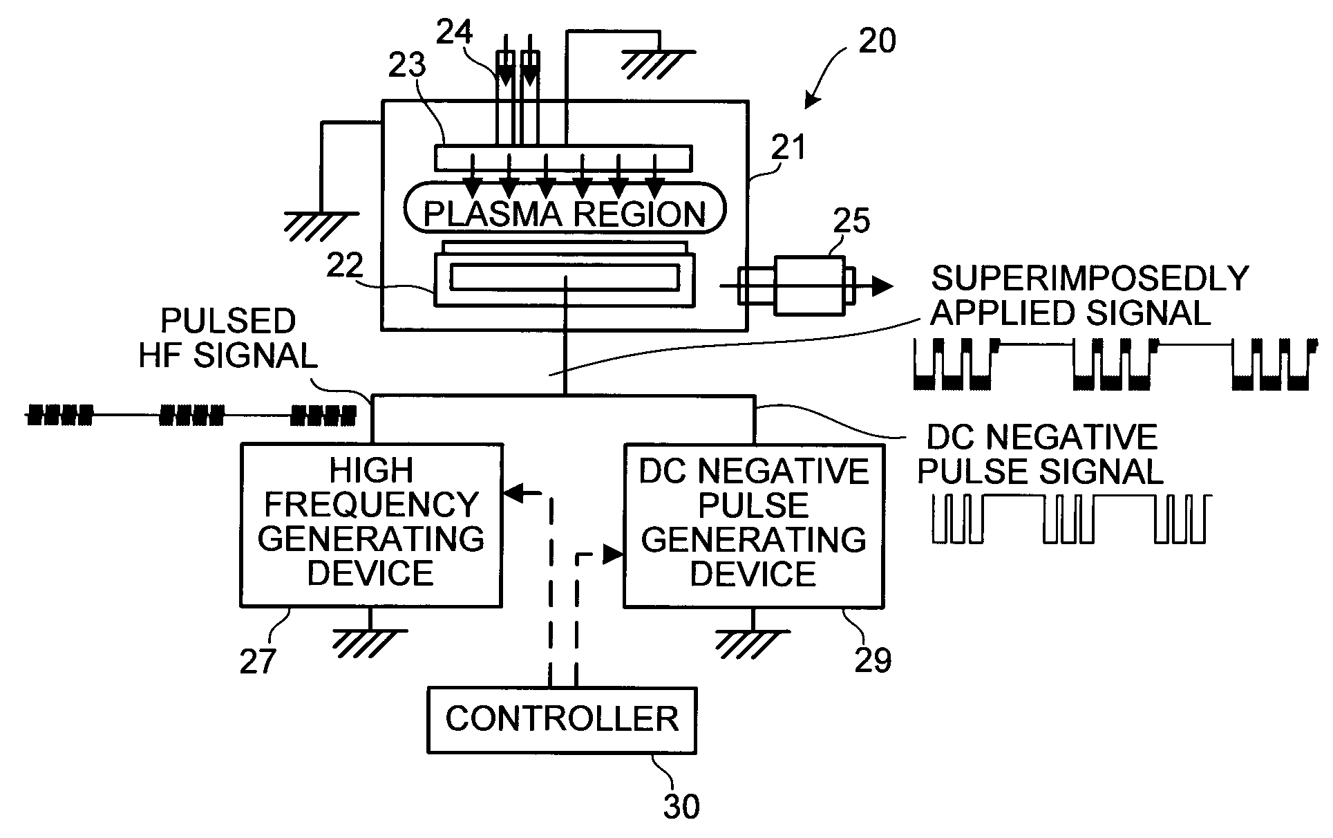
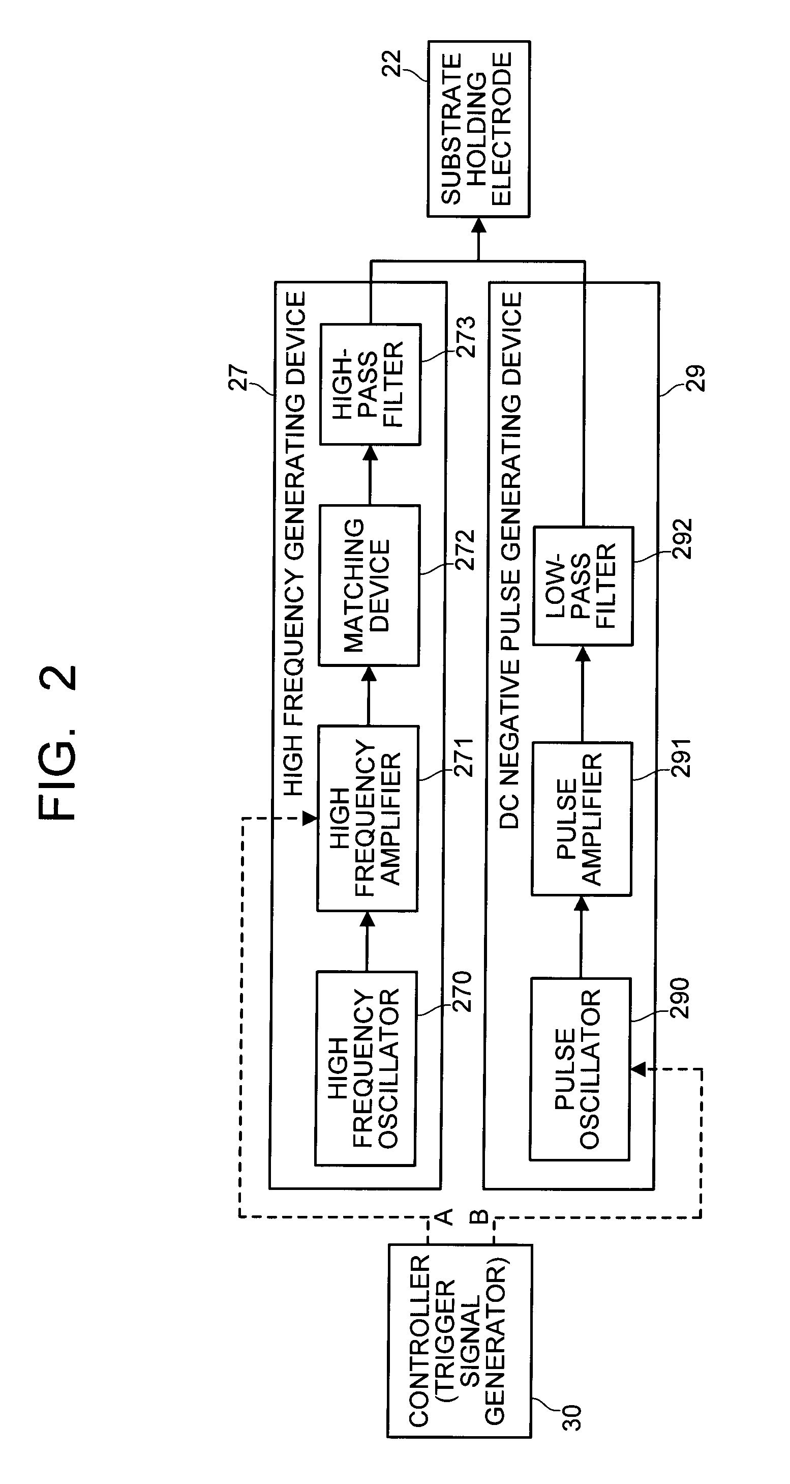
[0041]Hereinafter, embodiments of a substrate plasma processing apparatus and a substrate plasma processing method according to the present invention will be explained with reference to the drawings. First, an embodiment of the substrate plasma processing apparatus will be explained with reference to FIG. 1.

[0042]As shown in FIG. 1, the substrate plasma processing apparatus 20 of this embodiment is a plasma processing apparatus of what is called a parallel plate type. In a chamber 21 capable of being evacuated to a predetermined degree of vacuum, a substrate holding electrode (high frequency (RF) electrode) 22 and a counter electrode 23 are arranged facing each other. A main surface of this substrate holding electrode 22 that faces the counter electrode 23 is structured to be capable of holding a substrate S to be subjected to processing. In the chamber 21, a gas introducing pipe 24 and an exhaust port 25 connected to a not-shown vacuum pump are provided. Then a gas to be used for g...


PUM

PropertyMeasurementUnit
Frequencyaaaaaaaaaa
Frequencyaaaaaaaaaa

Abstract

A substrate plasma processing apparatus includes a substrate holding electrode and a counter electrode which are arranged in a chamber, a high frequency generating device which applies a high frequency of 50 MHZ or higher to the substrate holding electrode, a DC negative pulse generating device which applies a DC negative pulse voltage in a manner of superimposing on the high frequency, and a controller controlling to cause intermittent application of the high frequency and cause intermittent application of the DC negative pulse voltage according to the timing of on or off of the high frequency.

Description

CROSS-REFERENCE TO THE APPLICATIONS[0001]This application is based upon and claims the benefit of priority from the prior Japanese Patent Application No. 2008-023066, filed on Feb. 1, 2008; the entire contents of which are incorporated herein by reference.BACKGROUND OF THE INVENTION[0002]1. Field of the Invention[0003]The present invention relates to a substrate plasma processing apparatus of what is called a parallel plate type and a substrate plasma processing method, in which an RF electrode and a counter electrode are arranged facing each other in a vacuum chamber and a substrate held on the RF electrode is processed with plasma generated between the electrodes.[0004]2. Description of the Related Art[0005]When wiring or the like is performed on a substrate such as a semiconductor wafer, it is necessary to perform minute processing on the substrate. For this purpose, conventionally a plasma processing apparatus using plasma has been used frequently.[0006]FIG. 11 is a diagram sche...

Claims


Application Information

Patent Timeline
IPC IPC(8): B44C1/22C23F1/08
CPCH01J37/32027H01J37/32091H01J37/32045H01L21/205H01L21/265H01L21/3065
Inventor UI, AKIOTAMAOKI, NAOKIICHIKAWA, TAKASHIHAYASHI, HISATAKAKAMINATSUI, TAKESHIHIMORI, SHINJIYAMADA, NORIKAZUOHSE, TAKESHIABE, JUN
Owner TOKYO ELECTRON LTD
Why Eureka
Try Eureka