Group lll-V compound semiconductor and a method for producing the same

a compound semiconductor and semiconductor technology, applied in semiconductor devices, nanooptics, electrical apparatus, etc., can solve the problems of significant brightness degradation, unproduced crystals sufficiently satisfying high quality, and unsatisfactory brightness of light-emitting devices disclosed in these documents, and achieve high brightness

Inactive Publication Date: 2009-08-13
SUMITOMO CHEM CO LTD
View PDF25 Cites 16 Cited by
  • Summary
  • Abstract
  • Description
  • Claims
  • Application Information

AI Technical Summary

Benefits of technology

[0009]An object of the present invention is to provide a group III-V compound semiconductor which is suitable used as a light-emitting device with high brightness. Another object of the invention is to provide a method for producing the above group III-V compound semiconductor.

Problems solved by technology

However, since the lattice constant and chemical characteristics of substrates are quite different from that of the compound semiconductor, crystals sufficiently satisfying high quality have not yet been produced.
The light-emitting devices disclosed in these documents are not satisfied in viewpoint of brightness.
In this method, during growing a p-GaN layer, the InGaN layer is broken to precipitate indium metal or indium nitride crystal, resulting in significant deterioration of brightness (Journal of Crystal Growth, 248, 498, 2003).

Method used


Image

  • Group lll-V compound semiconductor and a method for producing the same
  • Group lll-V compound semiconductor and a method for producing the same

Examples


example 1

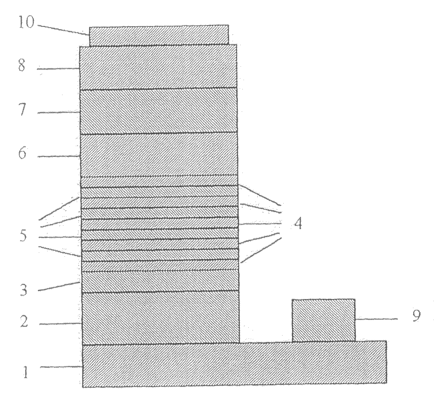
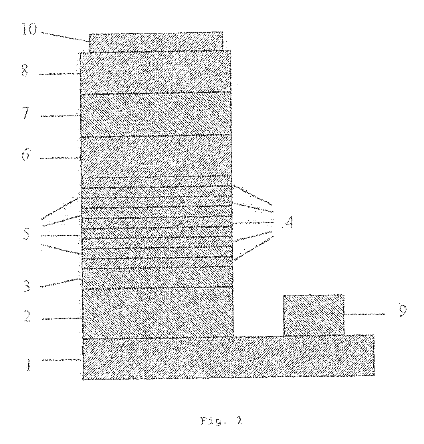
[0082]The low-temperature-grown GaN buffer layer was grown on C-face sapphire at 490° C. supplying TMG and ammonia as the raw materials and hydrogen as the carrier gas.

[0083]After TMG supply being once ceased, the temperature was raised up to 1090° C. and then TMG, ammonia and silane as the raw materials and hydrogen as the carrier gas were supplied to grow an n-type GaN layer having a thickness of 3 μm, followed by supply of silane being ceased to grow an undoped GaN layer having a thickness of 300 nm. After ceasing supply of TMG and silane and then being cooled down to 785° C., TEG and ammonia as the raw materials and nitrogen as the carrier gas were supplied to grow a GaN layer having a thickness of 100 nm, and then followed by repeating the procedure 5 times, the procedure that TEG, TMI and ammonia as the raw materials and nitrogen as the carrier gas were supplied under the pressure of 50 kPa to grow a InGaN layer having a thickness of 3 nm and a GaN layer having a thickness of ...

example 2

[0089]An LED was obtained by the same operation as in Example 1 except the thickness of the p-type GaN layer changed to 450 nm. The LED was estimated under the same conditions as that of Example 1. The results are shown in Table 1.

example 3

[0090]An LED was obtained by the same operation as in Example 1 except the thickness of the p-type GaN layer changed to 300 nm. The LED was estimated under the same conditions as that of Example 1. The results are shown in Table 1.

Reference 1

[0091]An LED was obtained by the same operation as in Example 1 except the thickness of the p-type GaN layer changed to 150 nm. The LED was estimated under the same conditions as that of Example 1. The results are shown in Table 2.


PUM


Abstract

A Group III-V compound semiconductor includes an n-type layer, a p-type layer, a p-type layer represented by a formula InaGabAlcN, having a thickness of not less than 300 nm, and a multiple quantum well structure which exists between the n-type layer and the p-type layer, has at least two quantum well structures including two barrier layers and a quantum well layer represented by a formula InxGayAlzN between the barrier layers; and a ratio of R/α of not more than 42.5%, wherein R is an average mole fraction of indium nitride in the quantum well layer, which is measured by X-ray diffraction, and α is a mole fraction of indium nitride calculated from a wavelength of light emitted from the group III-V compound semiconductor due to current injection.

Description

TECHNICAL FIELD[0001]The present invention relates to a group III-V compound semiconductor having a p-type layer represented by a formula InaGabAlcN (a+b+c=1, 0≦a<1, 0<b≦1, 0≦c<1) and a quantum well structure including barrier layers and a quantum well layer represented by a formula InxGayAlzN (x+y+z=1, 0<x<1, 0<y<1, 0≦z<1) between the barrier layers.BACKGROUND ART[0002]A group III-V compound semiconductor represented by a formula IndGaeAlfN (d+e+f=1, 0≦d≦1, 0≦e≦1, 0≦f≦1) is currently used as a light-emitting device which emits colors of green, blue, violet or ultra violet.[0003]The white-light-emitting devices combined with light-emitting materials and fluorescent materials have been studied to apply to backlights or lightning. Since specific crystals containing indium nitride, for example, enable to change the wavelength of light emission by changing indium nitride (InN) mole fraction thereof, they are useful as a display device or a light source exciting f...

Claims


Application Information

Patent Timeline
Patent Type & Authority Applications(United States)
IPC IPC(8): H01L31/00H01L33/00H01L21/00H01L21/20H01L33/06H01L33/32
CPCB82Y20/00H01L33/32H01L33/06H01L33/007
Inventor SASAKI, MAKOTOTAKADA, TOMOYUKI
Owner SUMITOMO CHEM CO LTD
Why Eureka
Try Eureka