Method for driving semiconductor device, and semiconductor device

a semiconductor device and semiconductor technology, applied in semiconductor devices, digital storage, instruments, etc., can solve the problems of data easily losing, difficult to form an inversion layer, and a large decrease in the speed of the latter charge injection, so as to accurately monitor the amount of written charges, uniform shape of the accumulated charge distribution, and variability in electrical characteristics

Inactive Publication Date: 2009-08-13
NEC CORP
View PDF3 Cites 4 Cited by
  • Summary
  • Abstract
  • Description
  • Claims
  • Application Information

AI Technical Summary

Benefits of technology

[0018]By using such method of detecting the amount of written charges, it is possible to accurately monitor the amount of written charges under each writing voltage condition, whereby, variability in electrical characteristics among elements can be resolved and the shape of the accumulated charge distribution can be made uniform.
[0019]According to the present invention, in a case of writing to one memory cell of the trap type non-volatile memory cell, the trap type non-volatile memory cell includes; the laminated insulating film, containing the charge accumulation layer, being formed on the semiconductor substrate where the source, drain and well regions are formed; and the first gate electrode being formed on the laminated insulating film,

Problems solved by technology

However, after the 90 nm-generation, a trap type memory, which uses a trap inside the insulating film in charge trapping, has come to attract attention, given the situation that thinning of the insulating film has become difficult in view of the problem of considering the aspect of securing the charge retention characteristic.
This happens because the work function in the vicinity of node 2 will change in a positive direction due to electron accumulation, which makes it difficult for an inversion layer to be formed.
As shown in FIG. 6, in the case when the accumulated electron distribution profile exhibits a precipitous form, the signal intensity will change over time in a high-temperature retention test due to the accumulated charges diffusing in such a way as to relax the self-electric field in the high-temperature retentio

Method used


Image

  • Method for driving semiconductor device, and semiconductor device
  • Method for driving semiconductor device, and semiconductor device
  • Method for driving semiconductor device, and semiconductor device

Examples


first example

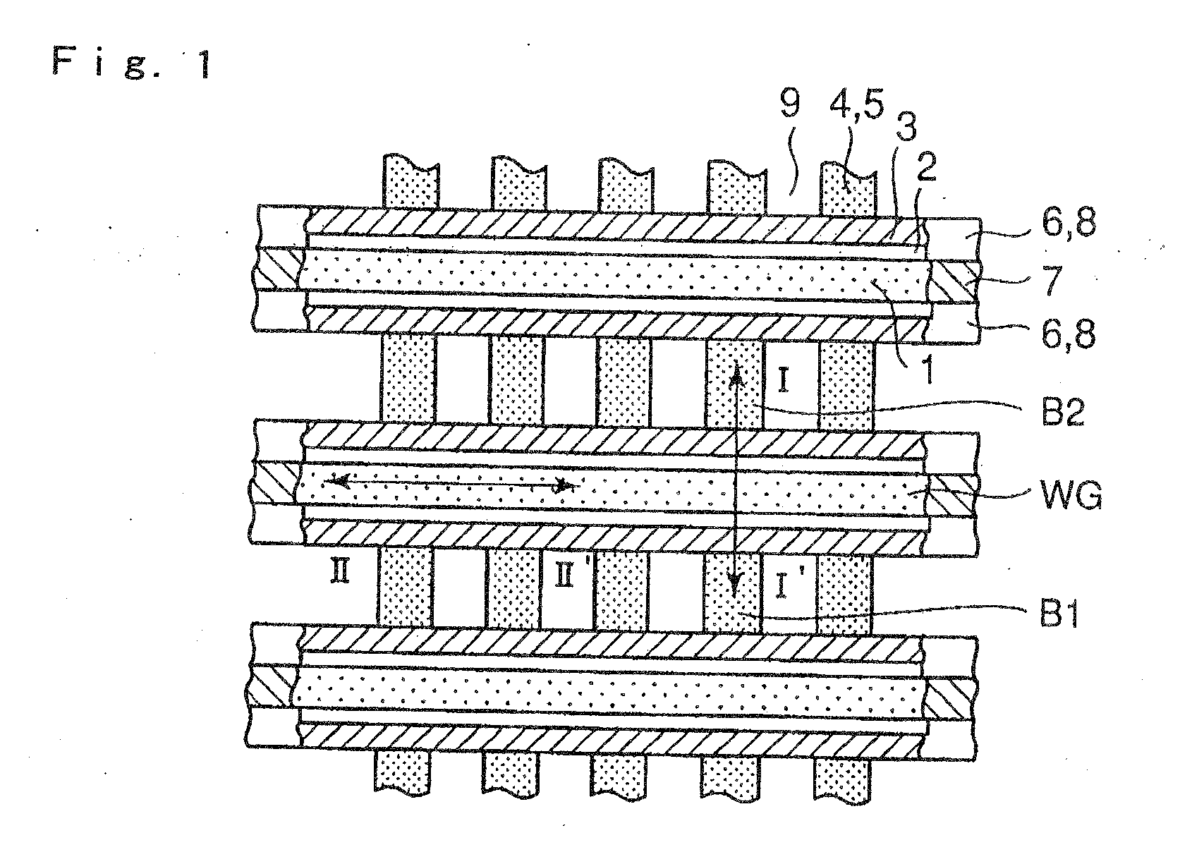
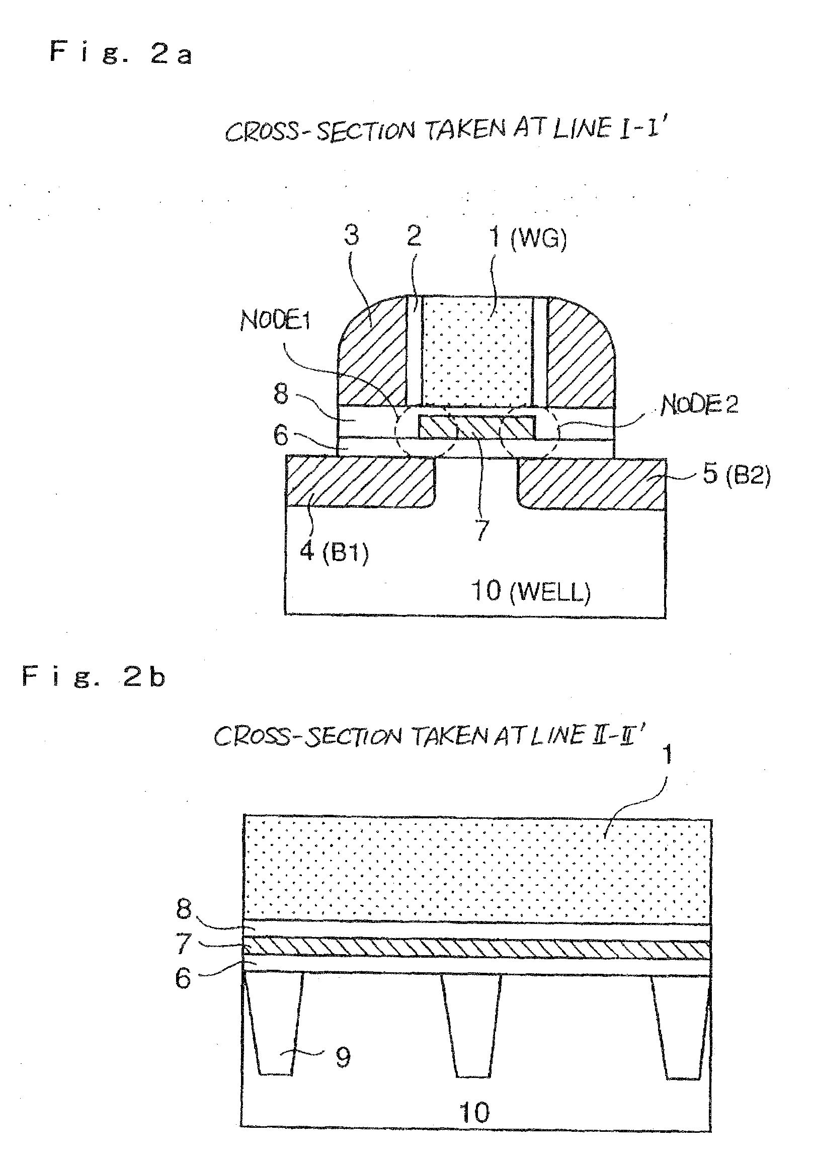
[0068]Next, a specific example of a case in which the method of driving a semiconductor device, according to the present invention, is applied to a SONOS type non-volatile memory, will be described in detail. A device structure used for the evaluation is the same as the one shown in FIG. 1 and FIG. 2. In this case, an oxide film formed by ISSG (in situ steam generation) is used as first gate insulating film 6, a CVD-Si3N4 film is used as charge accumulation film 7, and an oxide film formed by oxidizing an upper part of the CVD nitride film is used as second gate oxide film 8. Film thicknesses of the upper oxide film, the nitride film and the lower oxide film directly underneath gate electrode 1 are 4 nm, 4 nm and 5 nm, respectively.

[0069]FIG. 14 shows a writing characteristic when writing (charge injection) to node 2 is carried out, while bit line B1 is taken as a source and bit line B2 is taken as a drain, and under a writing condition (writing condition in the related art) where; ...

second example

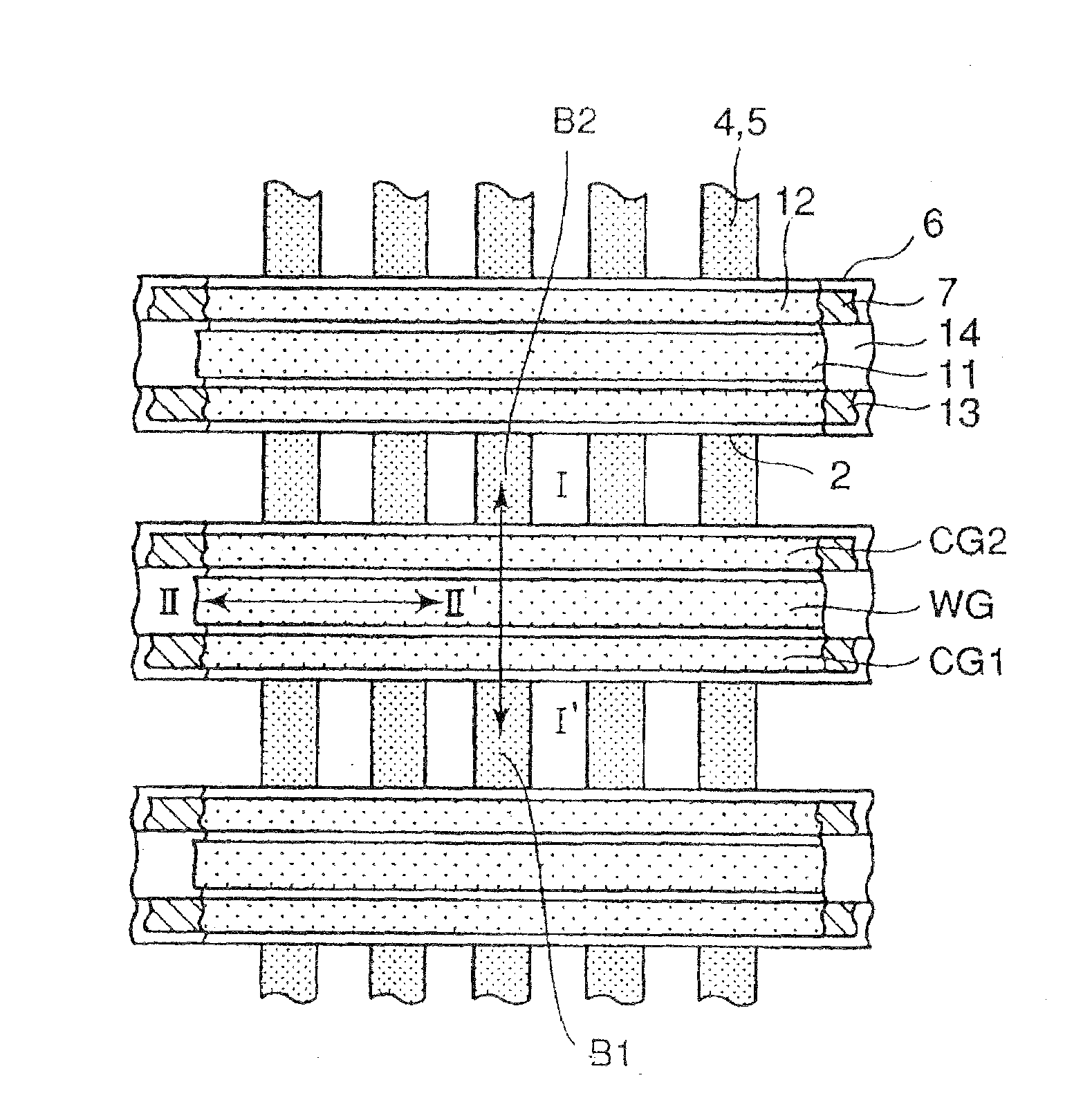
[0077]Now, a case in which the method of driving a semiconductor device, according to the present invention, is applied to a TWINMONOS type trap memory will be described in detail.

[0078]FIG. 17 is a plane view showing the TWINMONOS type trap memory. FIG. 18a is a sectional view taken at line I-I′ in FIG. 17 and FIG. 18b is a sectional view taken at line II-II′ in FIG. 17.

[0079]In the case of the TWINMONOS type trap memory, control gates 12 (CG1 and CG2) are arranged on both sides of word gate (WG) through inter-gate insulating films 13, respectively. Control gates 12 configure a pair of first gate electrodes while word gate 11 sandwiched in between control gates 12 is configures a second electrode.

[0080]Underneath each control gate 12, first gate insulating film 6, charge accumulation film 7 and second gate insulating film 8 are being formed. A charge accumulation region positioned underneath control gate CG1 will be node 1, and a charge accumulation region positioned underneath con...


PUM


Abstract

In a case of writing to a trap type non-volatile memory cell that includes: a laminated insulating film, containing a charge accumulation layer, that is formed on a semiconductor substrate where source, drain and well regions are formed; and a first gate electrode formed on the laminated insulating film, charge injections that are carried on a single memory node multiple times under two or more different writing conditions, the writing condition is a combination of a well voltage applied to the well, a drain voltage applied to the drain and a gate voltage is applied to the first gate. Thereby, it is possible to form a trapezoid-shaped electron distribution in the charge accumulation layer, and thus prevent the charge retention characteristic from deteriorating.

Description

TECHNICAL FIELD[0001]The present invention relates to a semiconductor device and a method of driving a semiconductor device, particularly to a method of driving a trap type non-volatile memory with excellent retention characteristic in terms of signal charge.BACKGROUND ART[0002]In the technology concerning miniaturization of flash memory, the mainstream development up till the 0.13 μm-generation of flash memories concerns reduction in the cell area and thinning of the insulating film using a floating gate (FG) type memory. However, after the 90 nm-generation, a trap type memory, which uses a trap inside the insulating film in charge trapping, has come to attract attention, given the situation that thinning of the insulating film has become difficult in view of the problem of considering the aspect of securing the charge retention characteristic. The trap type memory shows advantages over the FG type memory in the aspect that it is successive in having a thinned tunnel oxide film and...

Claims


Application Information

Patent Timeline
IPC IPC(8): G11C16/06G11C11/34H01L29/792
CPCG11C16/0466G11C16/10H01L27/115H01L29/7923H01L29/42344H01L29/42348H01L29/66833H01L27/11568H10B43/30H10B69/00
Inventor TERAI, MASAYUKI
Owner NEC CORP
Why Eureka
Try Eureka