
Current mirror circuit and optical receiver circuit using the same

a current mirror and optical receiver technology, applied in the direction of electromagnetic transmission, photometry using electric radiation detectors, transmission, etc., can solve the problem of low voltage gain of mosfets, insufficient bias voltage for pd in case of higher optical powers, and difficult to get satisfactory current mirror characteristics. achieve the effect of reducing gain and output impedance and operating stably

Active Publication Date: 2009-08-13
SUMITOMO ELECTRIC IND LTD
View PDF4 Cites 11 Cited by
  • Summary
  • Abstract
  • Description
  • Claims
  • Application Information

AI Technical Summary

Benefits of technology

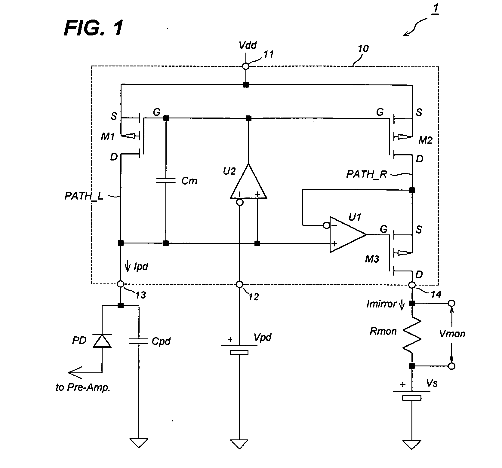
[0010]The current mirror circuit of the invention may further provide a third transistor, first and second differential amplifiers, and second input terminal. The second input terminal receives a reference voltage, and the second differential amplifier reflects this reference voltage to the first output terminal by a function of the virtual short circuit between the inverting and the non-inverting inputs of the differential amplifier, while, the first differential amplifier reflects this reference voltage reflected in the first output terminal to the second transistor. The third transistor, which is driven by the first differential amplifier, absorbs the difference between the reference voltage reflected in the second transistor and the voltage drop caused in the sensing resistor by the mirror current. Thus, the first and second transistors are biased substantially in the same condition and the reference voltage may be reflected in the first output terminal independent of the photocurrent flowing in the first transistor, which maintains the bias voltage applied to the PD to be substantially constant.
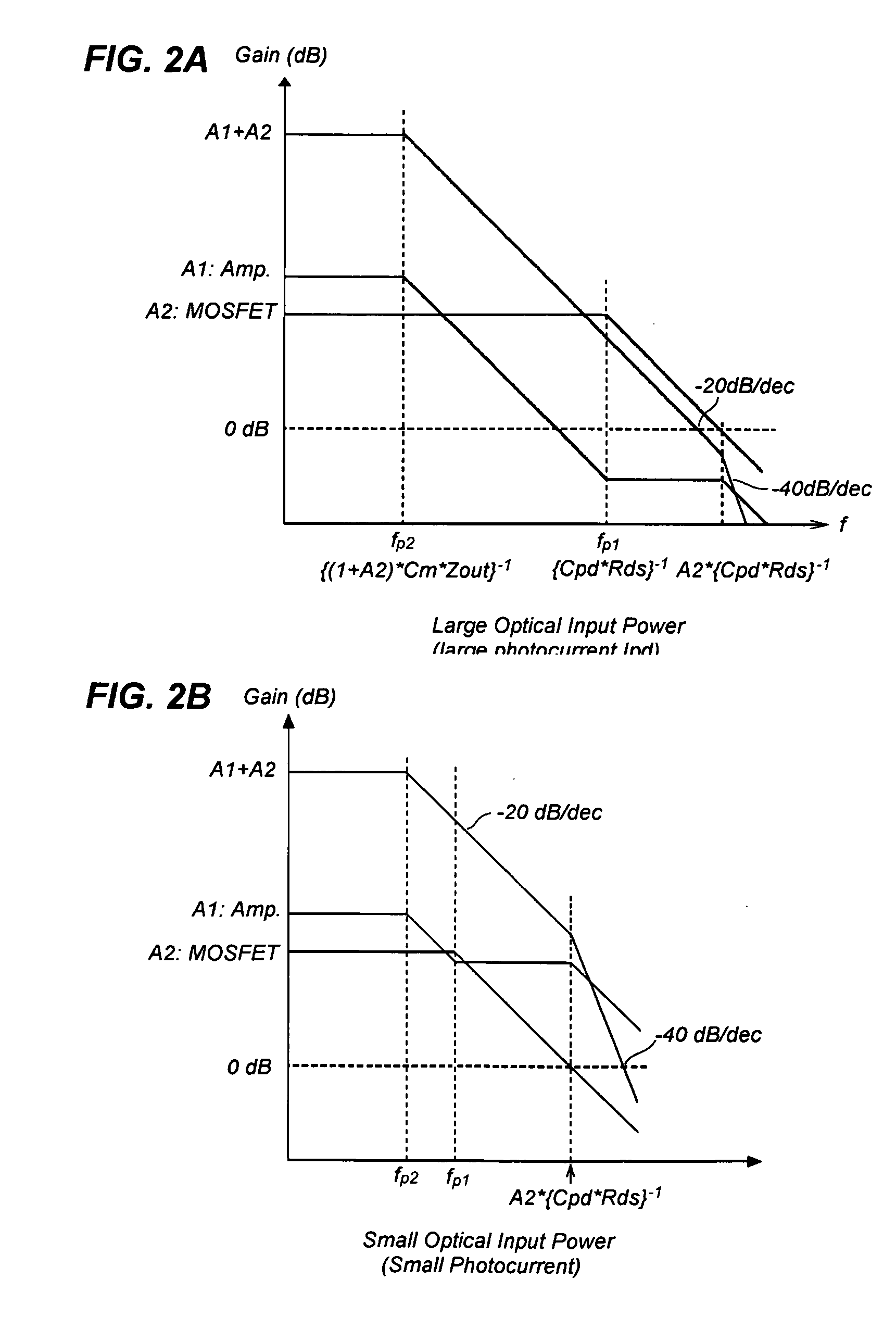
[0011]The second differential amplifier and the first transistor constitute a feedback loop to reflect the reference voltage to the first output terminal. In order to operate the feedback loop stably, the second differential amplifier of the invention provides a function to vary the gain and the output impedance thereof dynamically. The second differential amplifier may reduce the gain and the output impedance only when the photocurrent is relatively small, which shifts the pole frequency formed by the miller capacitor between the output of the second differential amplifier and the first output terminal and the output impedance toward higher frequency. Thus, the loop gain of the feedback loop has a slope of −20 dB / dec at a frequency where the loop gain is 0 dB, which means that the feedback loop may operate stably.

Problems solved by technology

However, because the dynamic range of the input optical power varies over 3-digits or more, from a few micro-decibel (dBμ) to a few milli-decibel (dBm) or more, the technique above described to detect the optical power through the voltage difference by the resistor has an inherent subject of the inaccuracy in a case of lower optical powers and the insufficient bias voltage for the PD in case of higher optical powers.
However, the MOSFETs has a lower voltage gain compared with that of the bipolar transistor and are hard to get a satisfactory current mirror characteristics.

Method used


Image

  • Current mirror circuit and optical receiver circuit using the same
  • Current mirror circuit and optical receiver circuit using the same
  • Current mirror circuit and optical receiver circuit using the same

Examples


Embodiment Construction

[0020]Next, preferred embodiments of an optical receiver and a current mirror circuit will be described as referring to accompanying drawings. In the description of the drawings, the same numerals or the same symbols will refer to the same elements without overlapping explanations.

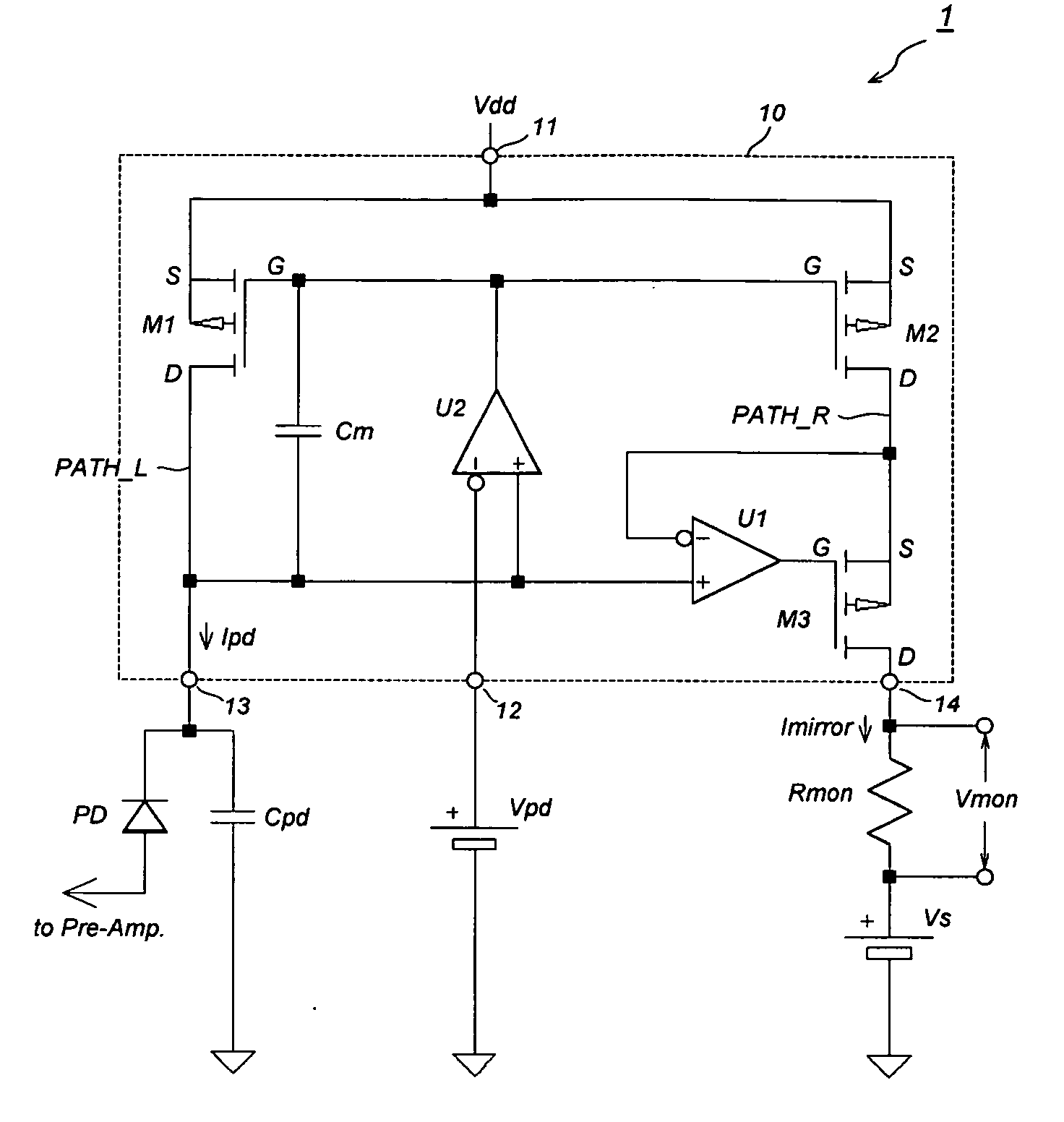
[0021]FIG. 1 is a circuit diagram of the optical receiver according to an embodiment of the present invention. The optical receiver 1, set between the positive power supply Vdd and the ground, includes a current mirror circuit 10, a PD, a reference voltage Vpd, and a sensing resistor Rmon. In the embodiment shown in FIG. 1, the current mirror circuit 10 includes a first current path PATH_L with a first p-MOSFET M1, a second current path PATH_R with a second p-MOSFET M2. These two p-MOSFETs, M1 and M2, operate so as to reflect the current flowing in the first current path PATH_L into a current flowing in the second current path PATH_R. The first current path PATH_L is inserted between the first input termin...


PUM


Abstract

A current mirror circuit and an optical receiver circuit implementing with the current mirror circuit are disclosed. The current mirror circuit provides two MOSFETs and two differential amplifiers. The MOSFETs are operated under the same bias condition even the power supply voltage decreases due to the virtual short-circuit characteristic between two inputs of the differential amplifier. One of the differential amplifiers provides a variable gain and output impedance characteristic to stabilize the feedback loop formed by this differential amplifier and one of the MOSFETs.

Description

CROSS-REFERENCE TO RELATED APPLICATION[0001]This application claims the benefit of U.S. Provisional Application No. 61 / 006,869, entitled “CMOS receive power monitoring circuit for optical receiver”, which is hereby incorporated by reference.BACKGROUND OF THE INVENTION[0002]1. Field of the Invention[0003]The present invention relates to an optical receiver with a current mirror circuit, in particular, the invention relates to an optical receiver with a current mirror circuit implementing with MOSFETs.[0004]2. Description of Prior Arts[0005]An optical receiver that receives an optical signal and converts it to a corresponding electrical signal generally provides a function to monitor an average power of the optical signal. In the optical receiver including a photodiode (hereafter denoted as PD), the circuit detects an average of the photocurrent generated in the PD by inserting a resistor in a bias line to the PD and by detecting a voltage difference in this resistor caused by the pho...

Claims


Application Information

Patent Timeline
Patent Type & Authority Applications(United States)
IPC IPC(8): H04B10/06
CPCG01J1/44H03F3/082H04B10/6911H03F2203/45674H03F3/45183
Inventor TOURETTE, BRUNO
Owner SUMITOMO ELECTRIC IND LTD
Learn More