Accelerator particle beam apparatus and method for low contaminate processing

Inactive Publication Date: 2009-08-20
SILICON GENERAL CORPORATION
View PDF102 Cites 38 Cited by
  • Summary
  • Abstract
  • Description
  • Claims
  • Application Information

AI Technical Summary

Benefits of technology

[0012]Numerous benefits are achieved using embodiments of the present invention. In particular, certain embodiments of the present invention may use a linear accelerator based on RFQ-linac and/or RFI technology that has been proven to be a cost effective way to obtain high-energy proton beam in 1 MeV to 5 MeV or higher. Alternative embodiments may employ a cyclotron particle accelerator. Alternative embodiments may employ other types of particle accelerators such as a DC electrostatic accelerator, an example of which is the DYNAMITRON proton accelerator available from Ion Beam Applications SA, Belgium) can also be used. Other DC electrostatic accelerators which may be used include Van de Graaff or Tandem Van de Graaff types. According to certain embodiments of the invention with proper dosage and temperature controls these high-energy H+ ions can be utilized for deep implantation down to 200 μm beneath a surface of a selected bulk semiconductor with minimum surface damage to form a desired cleave region thereof. Subsequently, through various controlled cleaving processes or direct layer transfer processes a free-standing thick film (with thickness about 200 μm or less) can be produced. Some embodiments of the invention can be used to produce free-standing single crystalline silicon or polycrystalline silicon thick films for manufacture photovoltaic cells. For example, implanting H+ ions at 5 MeV into silicon, would generate an approximate cleave depth of 220 μm. Some other embodiments of the present invention provide a method of introducing high energy particles for
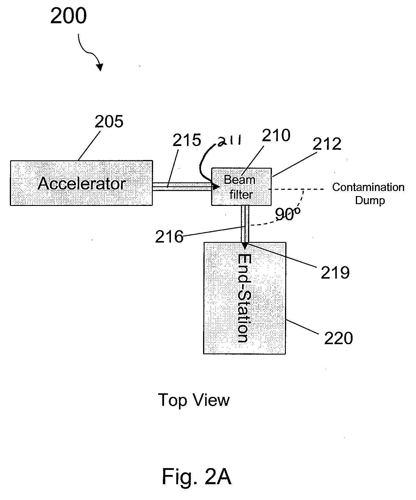
 ion impla

Problems solved by technology

Unfortunately, such petroleum sources have become depleted and have lead to other problems.
Although effective, these solar cells still have many limitations.
These materials are often difficult to manufacture.
Although these plates may be formed effectively, they do not possess optimum properties for highly effective solar cells.
Such single crystal silicon is, however, expensive and is also difficult to use for solar applications in an efficient and cost effective manner.
Additionally, both polysilicon and single-crystal silicon materials suffer from material losses during

Method used


Image

  • Accelerator particle beam apparatus and method for low contaminate processing
  • Accelerator particle beam apparatus and method for low contaminate processing
  • Accelerator particle beam apparatus and method for low contaminate processing

Examples


Embodiment Construction

[0026]Embodiments in accordance with the present invention relate generally to techniques including a method and a structure for forming substrates using layer transfer. More particularly, the present invention provides a method and system using a linear accelerator particle beam with low contaminate process for the manufacture of thick free-standing semiconductor films for a variety of applications including photovoltaic cells. But it will be recognized that the invention has a wider range of applicability; it can also be applied to other types of applications such as for three-dimensional packaging of integrated semiconductor devices, photonic or optoelectronic devices, piezoelectronic devices, flat panel displays, microelectromechanical systems (“MEMS”), nano-technology structures, sensors, actuators, integrated circuits, biological and biomedical devices, and the like.

[0027]FIG. 1 is a simplified diagram illustrating a system using an apparatus such as a linear acceleration appa...


PUM


Abstract

A system of introducing a particle beam such as a linear accelerator particle beam for low contaminate processing. The system includes an accelerator apparatus configured to generate a first particle beam including at least a first ionic specie in an energy level of 1 MeV to 5 MeV or greater. Additionally, the system includes a beam filter coupled to the linear accelerator apparatus to receive the first particle beam. The beam filter is in a first chamber and configured to generate a second particle beam with substantially the first ionic specie only. The first chamber is associated with a first pressure. The system further includes an end-station including a second chamber coupled to the first chamber for extracting the second particle beam. The second particle beam is irradiated onto a planar surface of a bulk workpiece loaded in the second chamber for implanting the first ionic specie. The second chamber is associated with a second pressure that is higher than the first pressure. Optional beam scanning can also be added between the beam filter and the end-station.

Description

CROSS-REFERENCE TO RELATED APPLICATION[0001]The instant nonprovisional patent application claims priority to U.S. Provisional Patent Application 60 / 997,684 filed Oct. 3, 2007, which is incorporated by reference in its entirety herein for all purposes.BACKGROUND OF THE INVENTION[0002]The present invention relates generally to technique including a method and a structure for forming substrates using a layer transfer technique. More particularly, the present invention provides a method and system using a linear accelerator particle beam or a particle beam from another type of accelerator such as a cyclotron or the like, with low contaminate process for the manufacture of thick free-standing semiconductor films for a variety of applications including photovoltaic cells. But it will be recognized that the invention has a wider range of applicability; it can also be applied to other types of applications such as for three-dimensional packaging of integrated semiconductor devices, photonic...

Claims


Application Information

Patent Timeline
IPC IPC(8): H01J27/00A61N5/00
CPCH01J37/3171H01J2237/022H01J2237/04735H01L21/76254H01J2237/18H01J2237/31705H01J2237/057
Inventor HENLEY, FRANCOIS J.LAMM, ALBERTBRAILOVE, ADAM
Owner SILICON GENERAL CORPORATION
Why Eureka
Try Eureka