

Organic thin film transistor
- Summary
- Abstract
- Description
- Claims
- Application Information
AI Technical Summary
Benefits of technology
Problems solved by technology
Method used
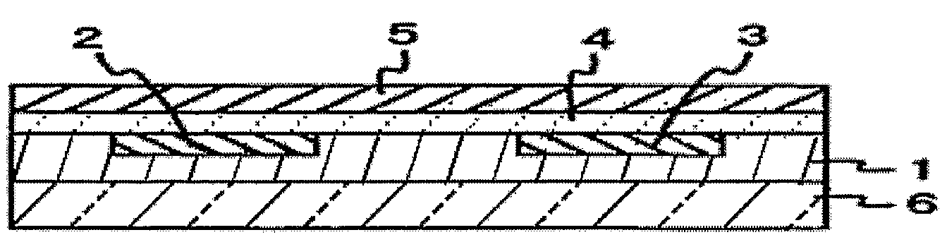
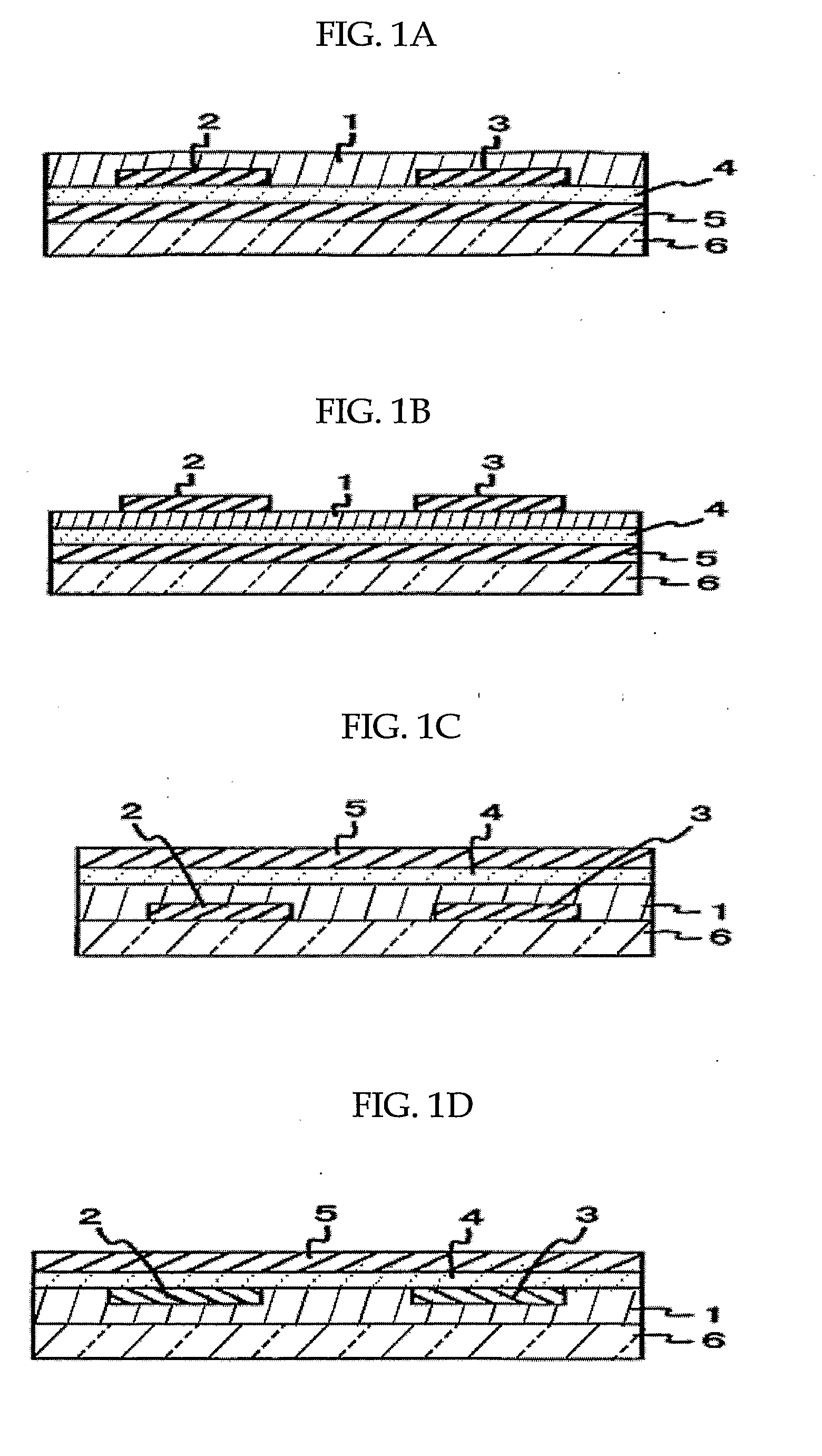
Image

Examples
synthesis example 1
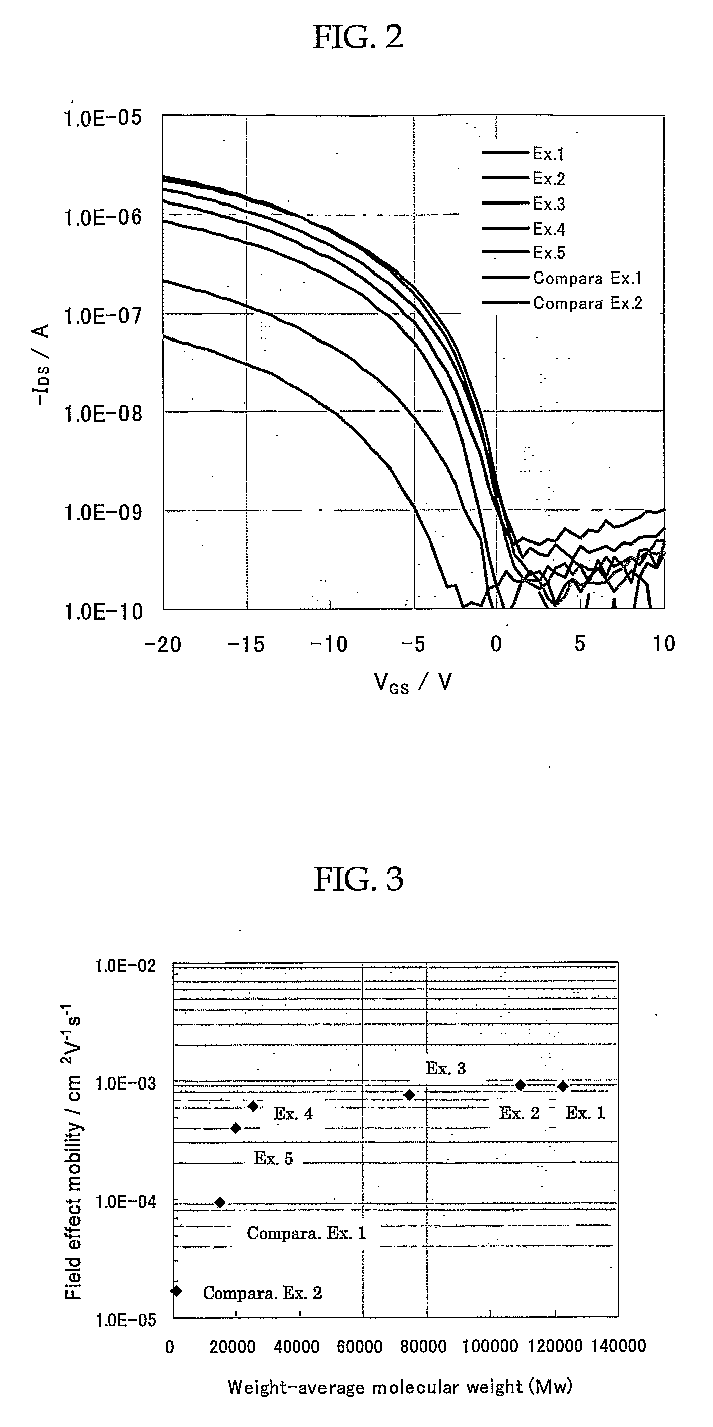
[0062]A 300-ml, four-necked flask was charged with 1.253 g (3.98 mmol) of dialdehyde, 2.243 g (3.98 mmol) of diphosphonate, and 10.5 mg (0.10 mmol) of benzaldehyde, and the air in the flask was then replaced by nitrogen gas, followed by the addition of 100 ml of tetrahydrofuran. To this resultant solution was added 12 ml of 1.0 mol / dm3 tetrahydrofuran solution of potassium t-butoxide, and stirred for 3 hours at room temperature. Then, 84 μl (0.398 mmol) of diethyl benzylphosphonate was added to the resultant solution and stirred for 2 hours. The reaction was quenched by the addition of about 1 ml of acetic acid. For purification, reprecipitation was then performed by use of dichloromethane and methanol to give 1.674 g of a polymer (total yield=74%).
[0063]The elemental analysis value (%) of the polymer was as follows: C, 84.02%; H, 8.22%; N, 2.52% (Calculated value (%): C, 84.12%; H, 7.92%; N, 2.42%).
[0064]The weight-average molecular weight (Mw) and number-average molecular weight (...
synthesis example 2
[0065]A 1000-ml, four-necked flask was charged with 8.48 g (26.9 mmol) of dialdehyde and 15.18 g (26.9 mmol) of diphosphonate, and the air in the flask was then replaced by nitrogen gas, followed by the addition of 800 ml of tetrahydrofuran. To this resultant solution was added 95 ml of 1.0 mol / dm3 tetrahydrofuran solution of potassium t-butoxide, and stirred for 10 minutes at 0° C. Then, 0.614 g (2.69 mmol) of diethyl benzylphosphonate was added to the resultant solution and stirred for 80 minutes. Furthermore, 0.571 g (5.38 mmol) of benzaldehyde was added to this solution and stirred for 2 hours. The reaction was quenched by the addition of about 5 ml of acetic acid. For purification, reprecipitation was then performed by use of tetrahydrofuran and methanol to give a polymer. Reprecipitation was again performed to purify the resultant polymer by use of tetrahydrofuran and acetone to give a polymer with a weight-average molecular weight (Mw) of 123,000.
synthesis example 3
[0066]In this Synthesis Example, 13.04 g of a polymer with a weight-average molecular weight (Mw) of 110,000 was produced in a similar manner described in Synthesis Example 2, with the exception that purification using tetrahydrofuran and acetone was omitted (total yield=85%)
PUM
| Property | Measurement | Unit |
|---|---|---|
| Molecular weight | aaaaa | aaaaa |
Abstract
Description
Claims
Application Information