
Eureka
For R&D, Eureka makes reading and utilizing patents & technical documents easy.
Eureka AIR
Designed for self-driven R&D workflows. Generate viable solutions, solve complex R&D challenges, empower your innovation with AI.

Eureka Materials
Designed for material experts only. Revolutionize your material R&D, from search, analyze, to developing new materials.

TechResearch
Generate reliable direction feasibility study reports for your R&D in just a few steps.

TechSeek
Discover and master advanced knowledge NOW. Basics, ideas, possibilities, all at once.

TechMind
As an expert in R&D Theories, TechMind can generates customized viable solutions instantly.

TechRisk
Analyze your overall solution with one click, know your potential R&D risks in advance.

TechMonitor
Get weekly tech updates, stay abreast of the latest tech innovations and key insights.
RF module
- Summary
- Abstract
- Description
- Claims
- Application Information
AI Technical Summary
Benefits of technology
Problems solved by technology
Method used
Image

Examples
first embodiment
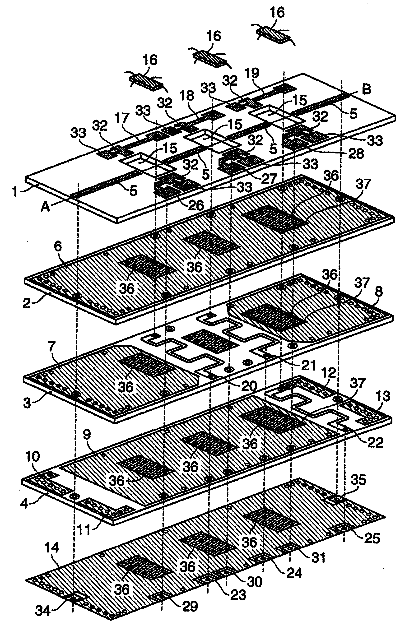
[0041]First, the detailed explanation will be given below regarding the present invention. FIG. 1 is a structural diagram of a radio-frequency wave module to which the present invention is applied. In FIG. 1, using a four-layer dielectric substrate, the radio-frequency wave module includes the following configuration components: A first-layer dielectric substrate 1, a second-layer dielectric substrate 2, a third-layer dielectric substrate 3, a fourth-layer dielectric substrate 4, metallic conductors 5 of a transmission-path-based distributed parameter element which are formed on the surface of the first-layer dielectric substrate 1 and through which a radio-frequency wave signal is propagated, a grounding-use metallic electrode 6 configuring a transmission-path-based distributed parameter element formed on the second-layer dielectric substrate 2, grounding-use metallic electrodes 7 and 8 formed on the third-layer dielectric substrate 3, grounding-use metallic electrodes 9, 10, 11, 1...
second embodiment
[0053]Next, the detailed explanation will be given below concerning the present invention. FIG. 4 is a structural diagram of a radio-frequency wave module to which the present invention is applied. In FIG. 4, using a four-layer dielectric substrate, the radio-frequency wave module includes the following configuration components: A first-layer dielectric substrate 1, a second-layer dielectric substrate 2, a third-layer dielectric substrate 3, a fourth-layer dielectric substrate 4, metallic conductors 5 of a transmission-path-based distributed parameter element which are formed on the surface of the first-layer dielectric substrate 1 and through which a radio-frequency wave signal is propagated, a grounding-use metallic electrode 6 configuring a transmission-path-based distributed parameter element formed on the second-layer dielectric substrate 2, grounding-use metallic electrodes 7 and 8 formed on the third-layer dielectric substrate 3, grounding-use metallic electrodes 9, 10, 11, 1...
third embodiment
[0064]Next, the detailed explanation will be given below concerning the present invention. FIG. 7 is a structural diagram of a radio-frequency wave module to which the present invention is applied. In FIG. 7, using a four-layer dielectric substrate, the radio-frequency wave module includes the following configuration components: A first-layer dielectric substrate 1, a second-layer dielectric substrate 2, a third-layer dielectric substrate 3, a fourth-layer dielectric substrate 4, metallic conductors 5 of a transmission-path-based distributed parameter element which are formed on the surface of the first-layer dielectric substrate 1 and through which a radio-frequency wave signal is propagated, matching circuits 38 each of which includes a lumped parameter element of a resistor, a capacitor, and an inductor, a grounding-use metallic electrode 6 configuring a transmission-path-based distributed parameter element formed on the second-layer dielectric substrate 2, grounding-use metallic...
PUM
 Abstract
Description
Claims
Application Information
 - R&D Engineer
- R&D Manager
- IP Professional
- Industry Leading Data Capabilities
- Powerful AI technology
- Patent DNA Extraction
Browse by: Latest US Patents, China's latest patents, Technical Efficacy Thesaurus, Application Domain, Technology Topic, Popular Technical Reports.
© 2024 PatSnap. All rights reserved.Legal|Privacy policy|Modern Slavery Act Transparency Statement|Sitemap|About US| Contact US: help@patsnap.com